Leave A Message
If you are interested in our products and want to know more details,please leave a message here,we will reply you as soon as we can.


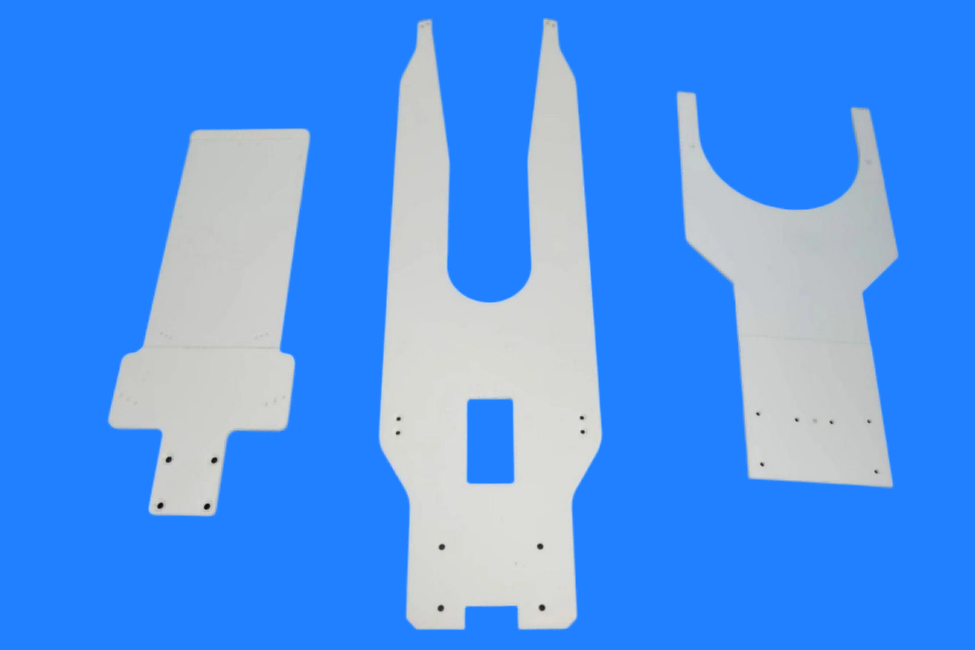
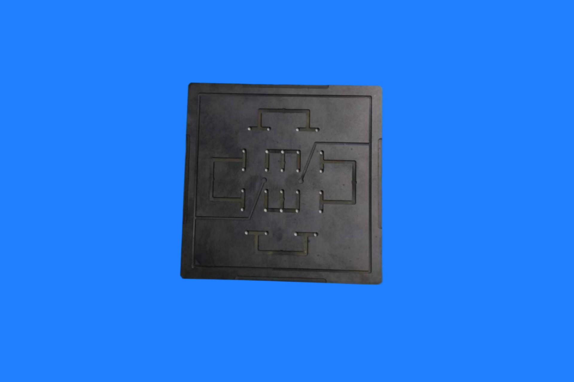
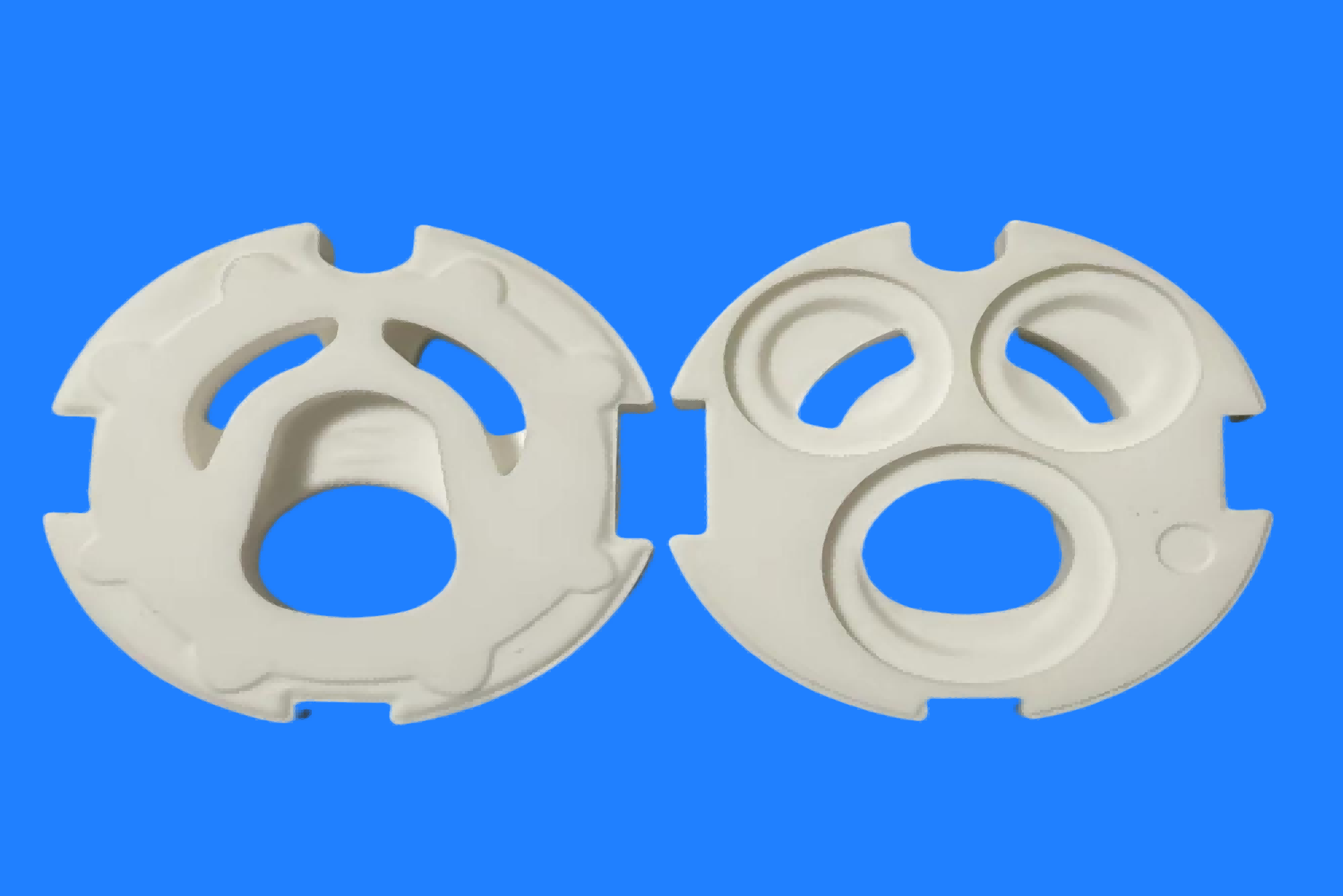
Yttria Stabilized Zirconia Ceramic Flow-splitting Nozzle Plate for Semiconductor
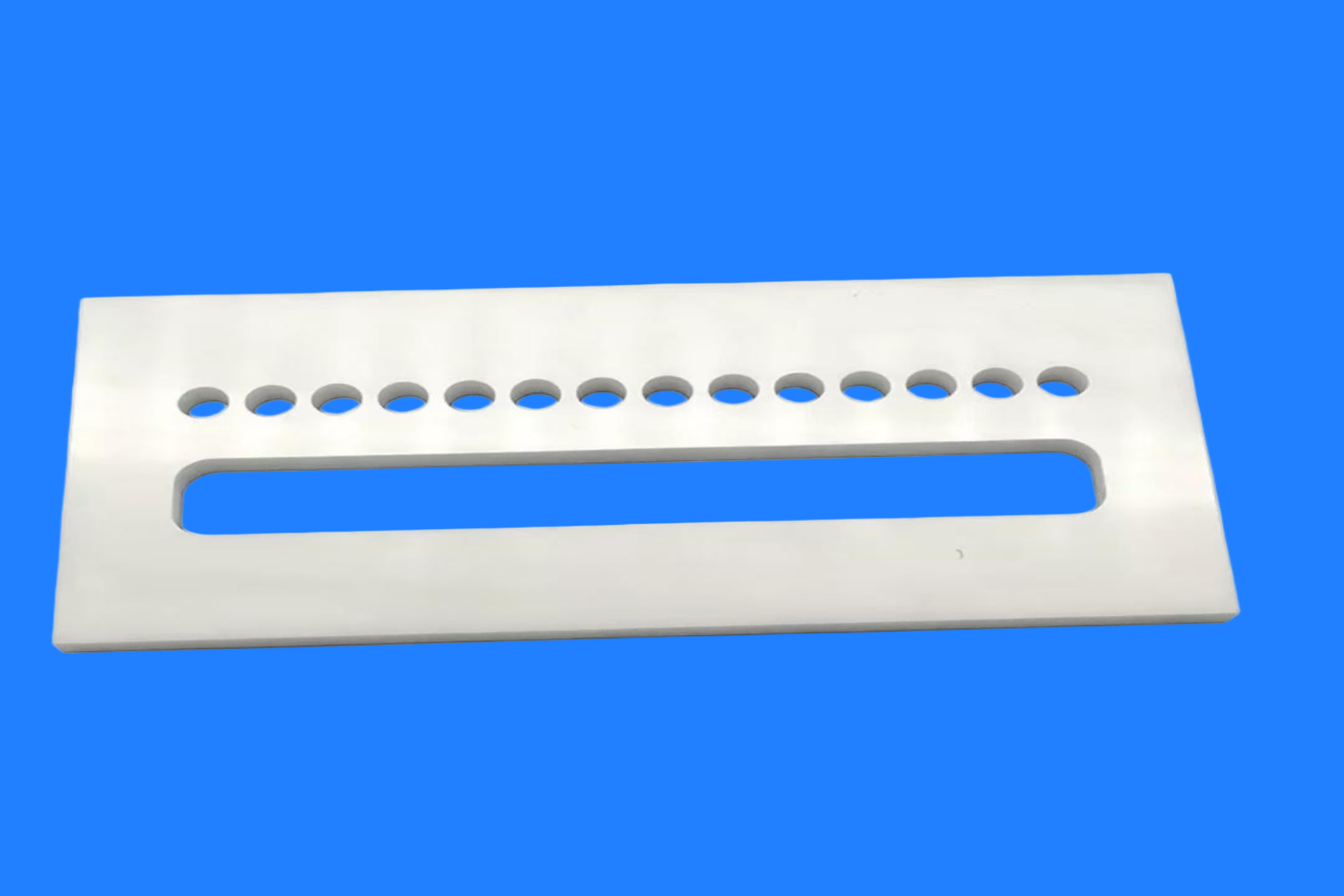
This Ysz Ceramic Nozzle Plate is manufactured using Yttria-Stabilized Zirconia (YSZ) precision ceramic material, with 3 mol% yttria-partially stabilized tetragonal zirconia polycrystal (3Y-TZP) serving as the core substrate. It is produced through isostatic pressing, high-temperature sintering, and precision machining. Designed for high-end applications such as semiconductor etching equipment, plasma processing chambers, and precision gas distribution systems, the plate combines ultra-high fracture toughness, excellent wear resistance, and superior thermal shock resistance with a precision micro-pore distribution structure. It ensures uniform, stable, and long-lasting gas distribution and plasma control, even under conditions involving highly corrosive plasma environments, high temperatures and pressures, and rapid thermal cycling.
Yttria Stabilized Zirconia Ceramic Flow-splitting Nozzle Plate for Semiconductor
Product Description
This Yttria Stabilised Zirconia Flow-splitting Nozzle Plate offers plasma corrosion resistance far superior to that of alumina ceramics. Its ultra-high toughness enables it to withstand extreme temperature fluctuations and high-velocity gas flow impacts without chipping or cracking. Featuring a mirror-polished inner nozzle surface and a low-porosity structure, the plate generates minimal particulates, meeting the stringent cleanroom production requirements for high-end chips. Equipped with an array of flow-splitting nozzles and elongated flow channels, it ensures the uniform delivery of highly corrosive fluorine- and chlorine-based process gases, thereby stabilizing wafer processing. Dimensions, nozzle apertures, and hole positions can be precision-customized to the micron level based on technical drawings. The plate offers significantly extended service life in harsh plasma environments and reduces equipment maintenance costs, providing a one-stop precision zirconia ceramic processing solution for global manufacturers of semiconductor and new energy equipment.
Product Core Advantages
1. Phase-transformation toughening mechanism: the "steel" of ceramics
Pure zirconia undergoes phase transitions—monoclinic ↔ tetragonal ↔ cubic—in response to temperature changes; these transitions are accompanied by a volume change of approximately 4–5%, which causes the material to crack. By precisely doping the material with 3 mol% yttrium oxide (Y₂O₃), the high-temperature tetragonal phase is stabilized down to room temperature, resulting in the formation of tetragonal zirconia polycrystals (TZP).Under stress, the metastable tetragonal phase within the material enables stress-induced phase transformation toughening; by absorbing the energy of crack propagation through this phase transformation, the fracture toughness of YSZ ceramics exceeds 7 MPa·m½—far surpassing traditional ceramics like alumina—earning it the reputation of "ceramic steel."
2.Ultra-high mechanical strength, capable of withstanding extreme operating conditions
Flexural strength: ≥900 MPa (3Y-TZP), ranking among the highest of all oxide ceramics
Compressive strength: ≥2200 MPa
Vickers hardness: ≥1300 HV, offering excellent wear resistance
Elastic modulus: approximately 220 GPa, comparable to steel, facilitating integration with metal structural components
Maintains structural integrity over extended periods, even under severe mechanical stress and plasma bombardment.
3.Precision microporous flow-distribution structure ensures uniform plasma distribution.
Utilizes precision laser drilling and CNC micromachining technologies; hole diameters range from 0.1 to 2.0 mm (customizable) with a positional accuracy of ±5 μm.
Optimized hole array layout ensures uniform gas/plasma distribution within the chamber, preventing localized over-etching or under-etching.
The flow-distribution plate features a precision-ground and polished surface with a roughness of Ra ≤ 0.1 μm, minimizing particle contamination and gas turbulence.
4.Excellent resistance to plasma corrosion
Demonstrates exceptional chemical inertness against fluorine-, chlorine-, and oxygen-based plasmas
In semiconductor etching processes (such as ICP, CCP, and RIE), it offers far superior resistance to halogen gas corrosion (e.g., CF₄, SF₆, Cl₂) compared to traditional materials like quartz and alumina; its low particle generation rate effectively reduces chamber contamination and wafer defects.
5.Excellent thermal shock resistance
Coefficient of thermal expansion: 10.3 × 10⁻⁶/°C (20–1000°C); good thermal compatibility with metal structural components
Thermal conductivity: 2.0–2.5 W/m·K; low thermal conductivity effectively reduces heat loss
Thermal shock resistance (ΔT): 280–350°C; capable of withstanding rapid heating and cooling cycles
Long-term service temperature: ≤850°C (structural components); capable of withstanding higher temperatures for short periods\
6.Precision Geometric Accuracy
Flatness: ≤5 μm (depending on dimensions)
Parallelism: ≤3 μm
Bore Diameter Tolerance: ±2 μm
Ensures a perfect fit with the chamber sealing surface, preventing gas leakage and cross-contamination.
Technical Specifications
| Material System | 3Y-TZP (3 mol% Y₂O₃-partially stabilized zirconia) |
| Chemical Composition | ZrO₂ ≥ 94.8%,Y₂O₃ 5.0–5.4% |
| Crystal Structure | primarily the tetragonal phase (t-phase), with a small amount of the cubic phase. |
| Density | 5.95–6.05 g/cm³ |
| Porosity | ≤0.5% (dense sintered body) |
| Flexural Strength | ≥900 MPa |
| Compressive Strength | ≥2200 MPa |
| Fracture Toughness | ≥7 MPa·m½ |
| Vickers Hardness | ≥1300 HV |
| Coefficient of Thermal Expansion (20–1000°C) | 10.3 ×10⁻⁶/℃ |
| Thermal Conductivity (25°C) | 2.0–2.5 W/m·K |
| Dielectric Constant (1 MHz) | 25–30 |
| Volume Resistivity (25°C) | >1×10¹⁴ Ω·cm |
| Maximum Operating Temperature | 850°C (long-term) |
| Thermal Shock Resistance (ΔT) | 280–350℃ |
| Surface Roughness | Ra ≤ 0.1 μm (polished surface) |
| Flatness | ≤5 μm |
| Micropore Size | 0.1–2.0 mm (customizable) |
| Hole Position Accuracy | ±5 μm |
| Standard Size | φ100–φ400 mm (customizable) |
| Thickness Range | 3–50 mm (customizable) |
Product Applications
1.Semiconductor Manufacturing
ICP/CCP plasma etching equipment: upper/lower electrode showerheads that evenly distribute etching gas and control plasma density distribution
PECVD/CVD equipment: gas distribution plates ensuring uniform deposition of reactant gases
Dry etching chambers: resistant to fluorine- and chlorine-based plasma corrosion, extending chamber maintenance intervals
Wafer cleaning equipment: chemically resistant flow-splitting and spraying components
2.Display Panel Manufacturing
OLED/LCD etching equipment: large-area gas distribution ensures etching uniformity across the panel.
Thin-Film deposition equipment: precision gas flow splitting controls film thickness uniformity.
3.Photovoltaics and New Energy
Solar cell etching: acid/alkali-resistant and highly wear-resistant flow distribution components
Fuel cells (SOFC): YSZ used as a solid electrolyte material for high-temperature gas distribution and electrode support
4.Precision Machining and Specialized Equipment
Sandblasting/plasma spraying nozzles: high hardness and wear resistance; service life far exceeds that of traditional metal nozzles.
High-Temperature Furnace Gas Distribution Systems: withstand ultra-high temperatures exceeding 2500°C (refractory-grade YSZ).
Product Series
| Series Name | Applicable Scenarios | Typical Specifications | Key Features |
| Etched Flow Distribution Plate | ICP/CCP plasma etching | φ200–φ400 mm | ultra-high plasma erosion resistance, low particle generation |
| Gas Distribution Plate | PECVD/CVD deposition | φ150–φ300 mm | precision hole array, gas uniformity ±3% |
| Electrode Protection Board | semiconductor Etching Machine Electrode | φ100–φ200 mm | high dielectric strength and resistance to arc erosion |
| Fire-resistant Distribution Llate | ultra-high temperature furnace / Metallurgy | customized | withstands temperatures above 2500°C and exhibits excellent thermal shock resistance. |
Quality Assurance
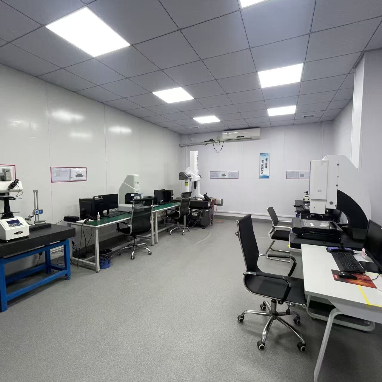
Inspection system:
Customized Services
We provide end-to-end customized solutions:
| Custom Dimensions | Services Offered |
| Ingredient Formula | 3Y-TZP / 5Y-PSZ / 8Y-FSZ / Mg-PSZ optional |
| Microporous Design | aperture size, hole spacing, hole shape (round/square/special-shaped), and array layout. |
| Surface Treatment | mirror polishing (Ra ≤ 0.05 μm), plasma spray coating, PVD/CVD coating |
| Structural Integration | precision bonding with metal flanges/ceramic bases; threaded or snap-fit interface design. |
| Dimensions and Specifications | maximum machinable size: 350 × 200 mm; thickness: 0.25–50 mm. |
Comparison with Competitor Materials
| Performance Indicators | YSZ(3Y-TZP) | Alumina (99.5%) | Quartz (SiO₂) | Aluminum nitride (AlN) |
| Flexural Strength | ≥900 MPa | ≥379 MPa | ~50 MPa | ≥300 MPa |
| Fracture Toughness | ≥7 MPa·m½ | ~4 MPa·m½ | ~1 MPa·m½ | ~3 MPa·m½ |
| Resistance to Plasma Corrosion | ★★★★★ | ★★★☆☆ | ★★★★☆ | ★★★☆☆ |
| Thermal Shock Resistance | ★★★★★ | ★★★☆☆ | ★★★★☆ | ★★★★☆ |
| Wear Resistance | ★★★★★ | ★★★★☆ | ★★★☆☆ | ★★★★☆ |
| Insulation Properties | ★★★★★ | ★★★★★ | ★★★★★ |
★★★☆☆ |
YSZ Ceramic Gas-Splitting Nozzle Plate—Leveraging the exceptional toughness of "ceramic steel" to provide long-life, high-reliability, and low-contamination plasma gas-splitting solutions for precision semiconductor manufacturing.
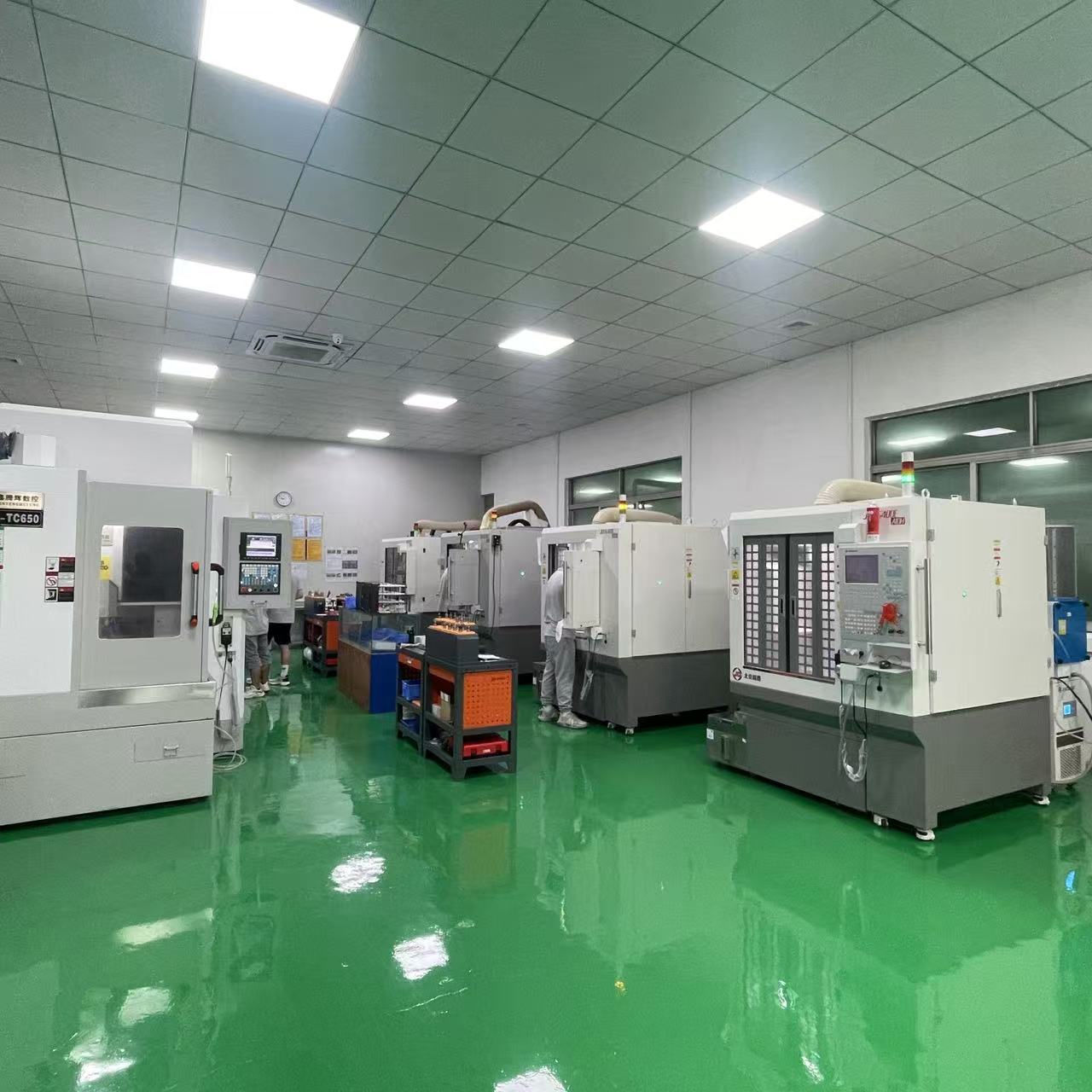
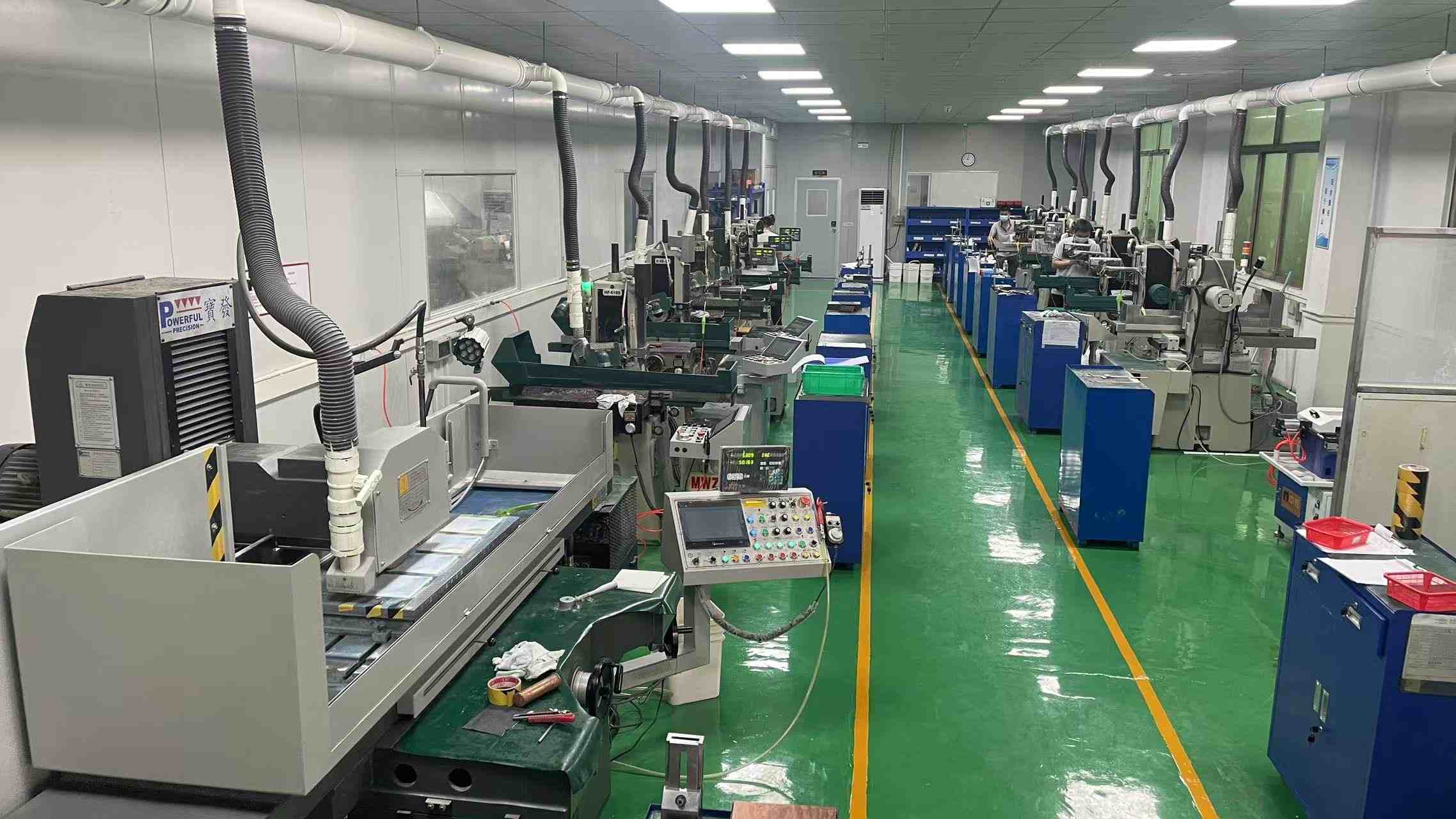
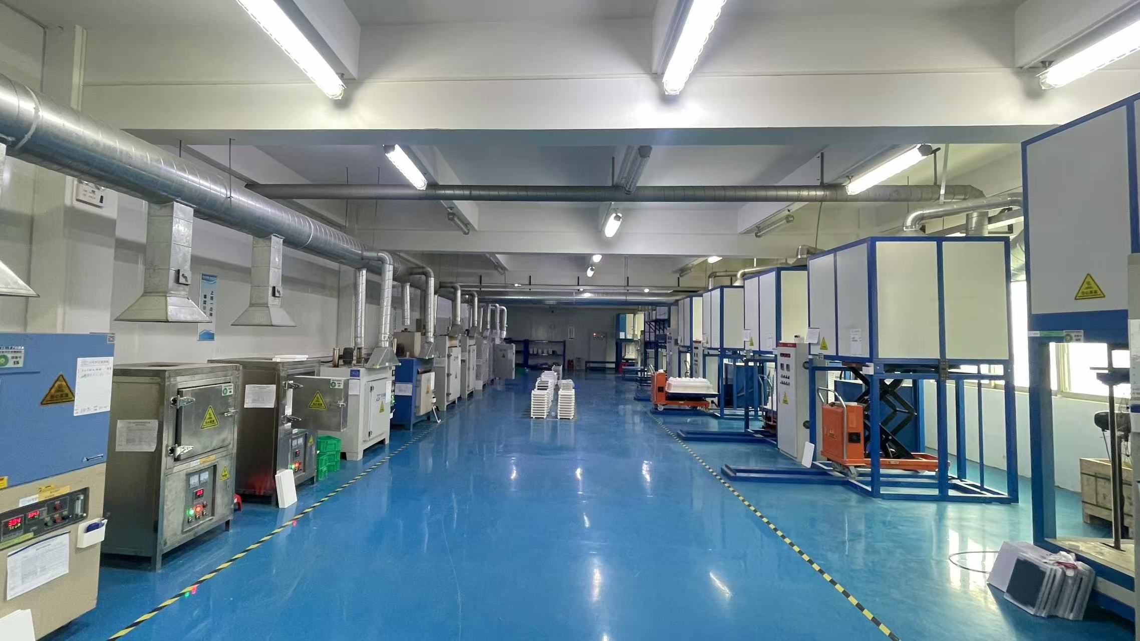
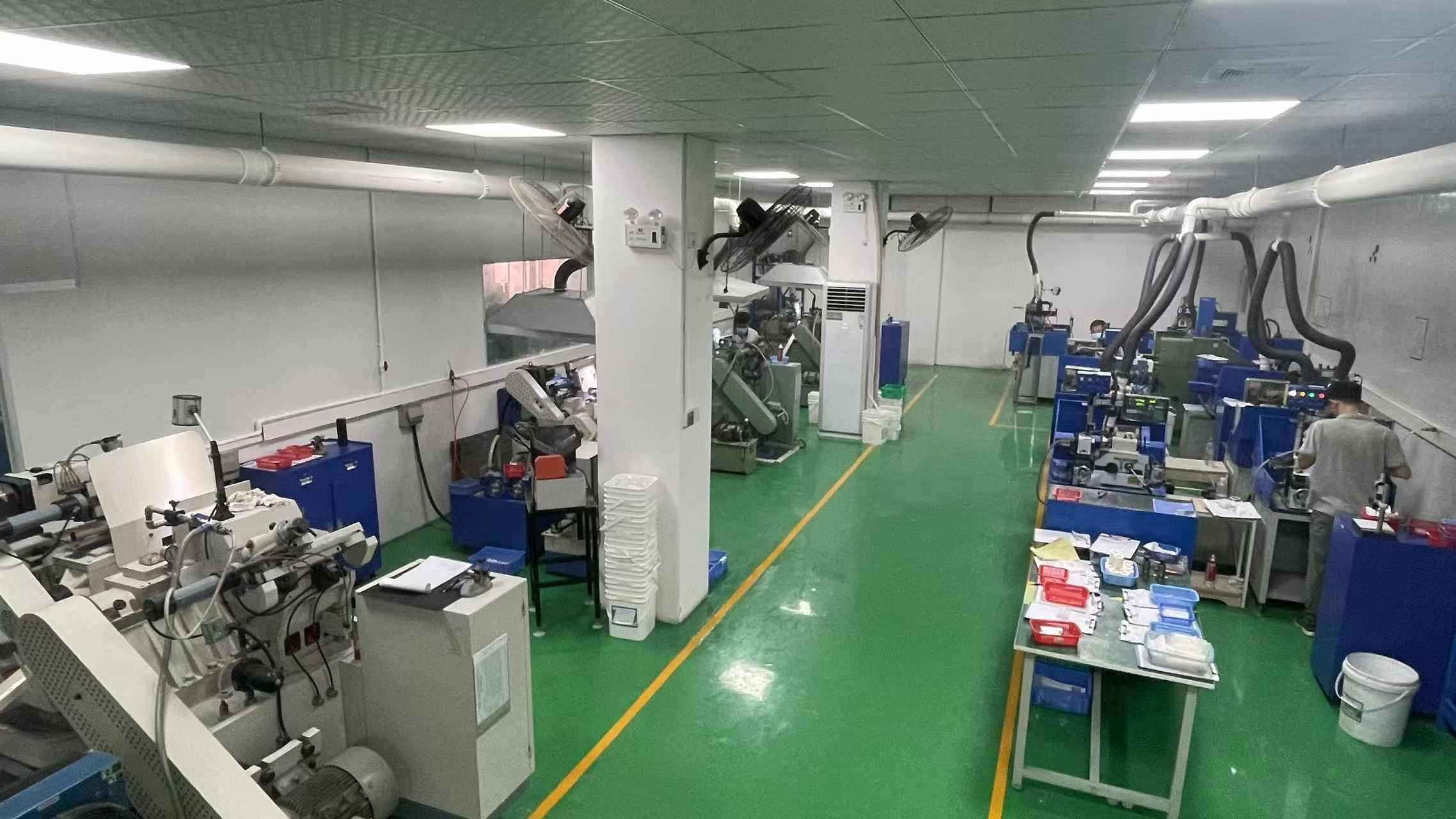
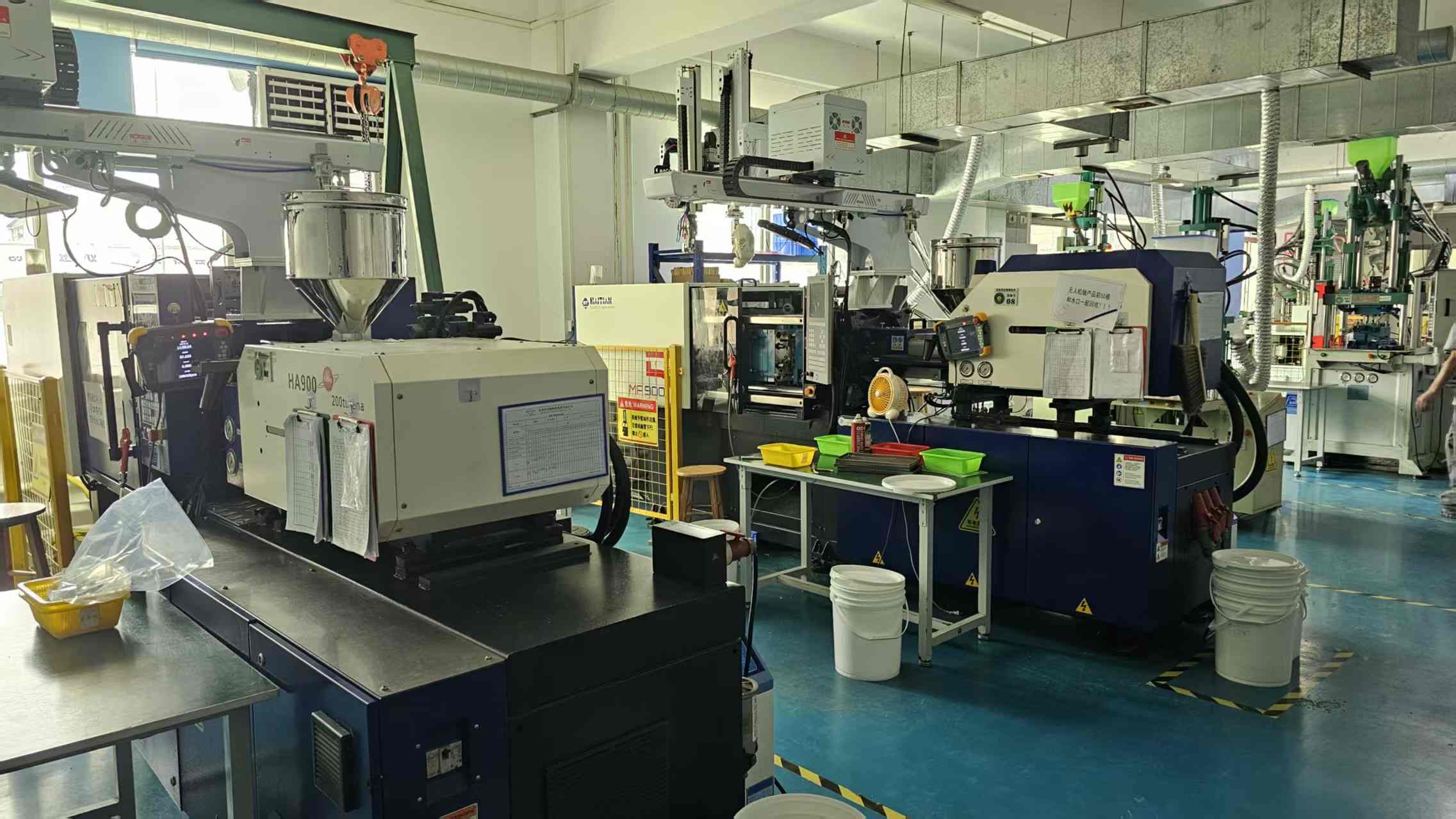
Our workshop
|
CNC Workshop |
Testing Room |
|
Surface grinding Workshop |
Sintering Workshop |
|
Circular Grinding Workshop |
Injection molding Machine Workshop |
Why choose us?
1.Customized R&D, rather than standard product adaptation
2.Deep control of materials science:Material Selection Based on Needs,Microstructure Optimization,Batch Consistency
3.Precision machining capability:Flatness can reach 0.001mm, parallelism 0.002mm, and roughness Ra 0.1μm.
FAQ
Q1: What products does your company offer?
We specialize in high-performance ceramics such as alumina and silicon nitride, providing insulators, structural components, wear-resistant parts, and customized solutions.
Q2: Can you customize non-standard parts?
Yes. We support processing based on provided drawings and collaborative technical development, offering a full-process service from design to mass production.
Q3: What about accuracy and delivery time?
Standard tolerance ±0.05mm, precision grade ±0.01mm; samples 7-15 days, bulk orders 20-30 days.
Q4: Main application areas?
Power, electronics, machinery, chemical, and aerospace industries.
Q5: Quality assurance measures?
Full-process quality inspection, providing material reports and performance test data, supporting third-party certification and testing.
Q6: Do you provide technical support?
We provide professional support such as material selection consultation, design optimization, and failure analysis.



 IPv6 network supported
Leave A Message
Scan to Wechat :

Scan to WhatsApp :