Leave A Message
If you are interested in our products and want to know more details,please leave a message here,we will reply you as soon as we can.


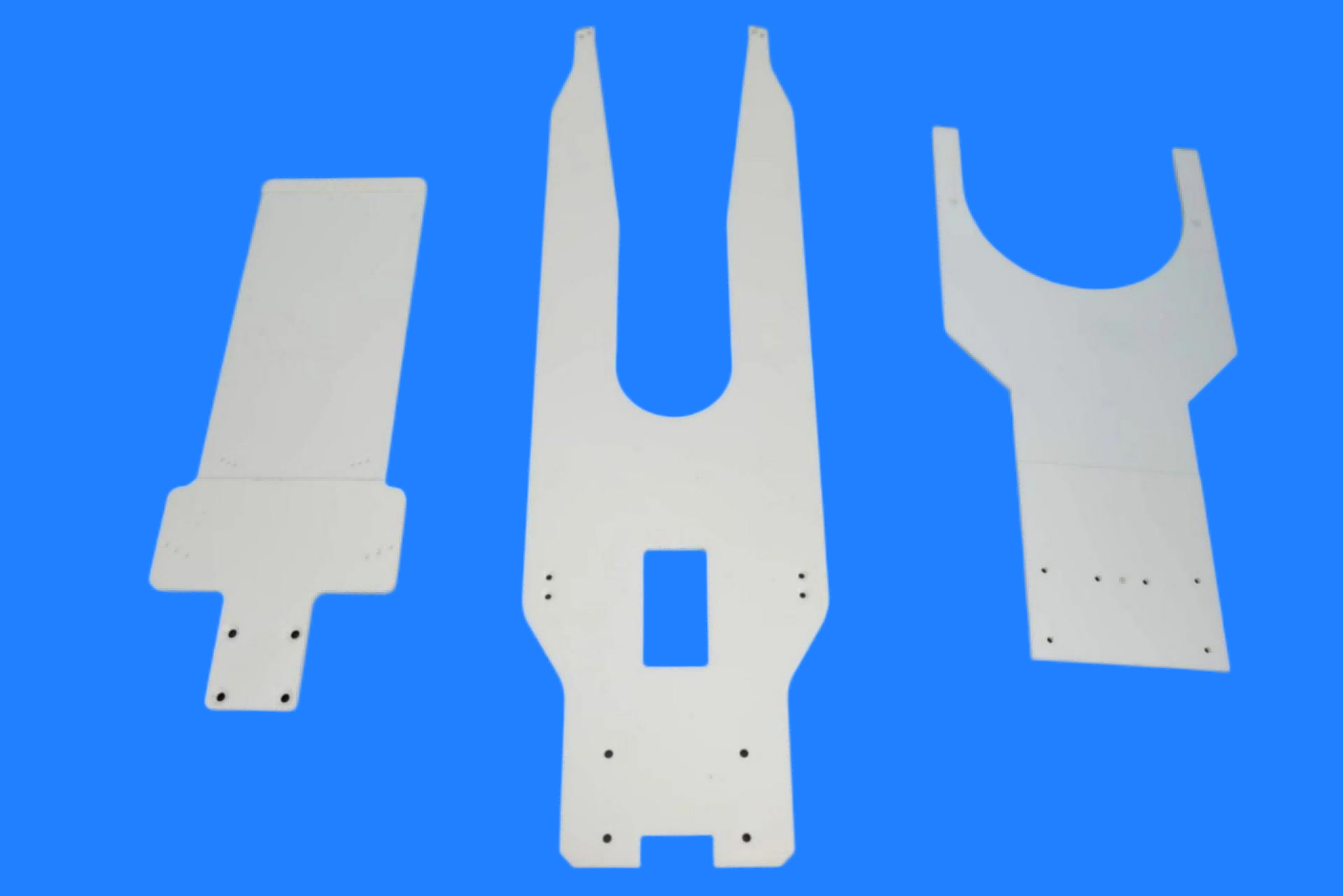
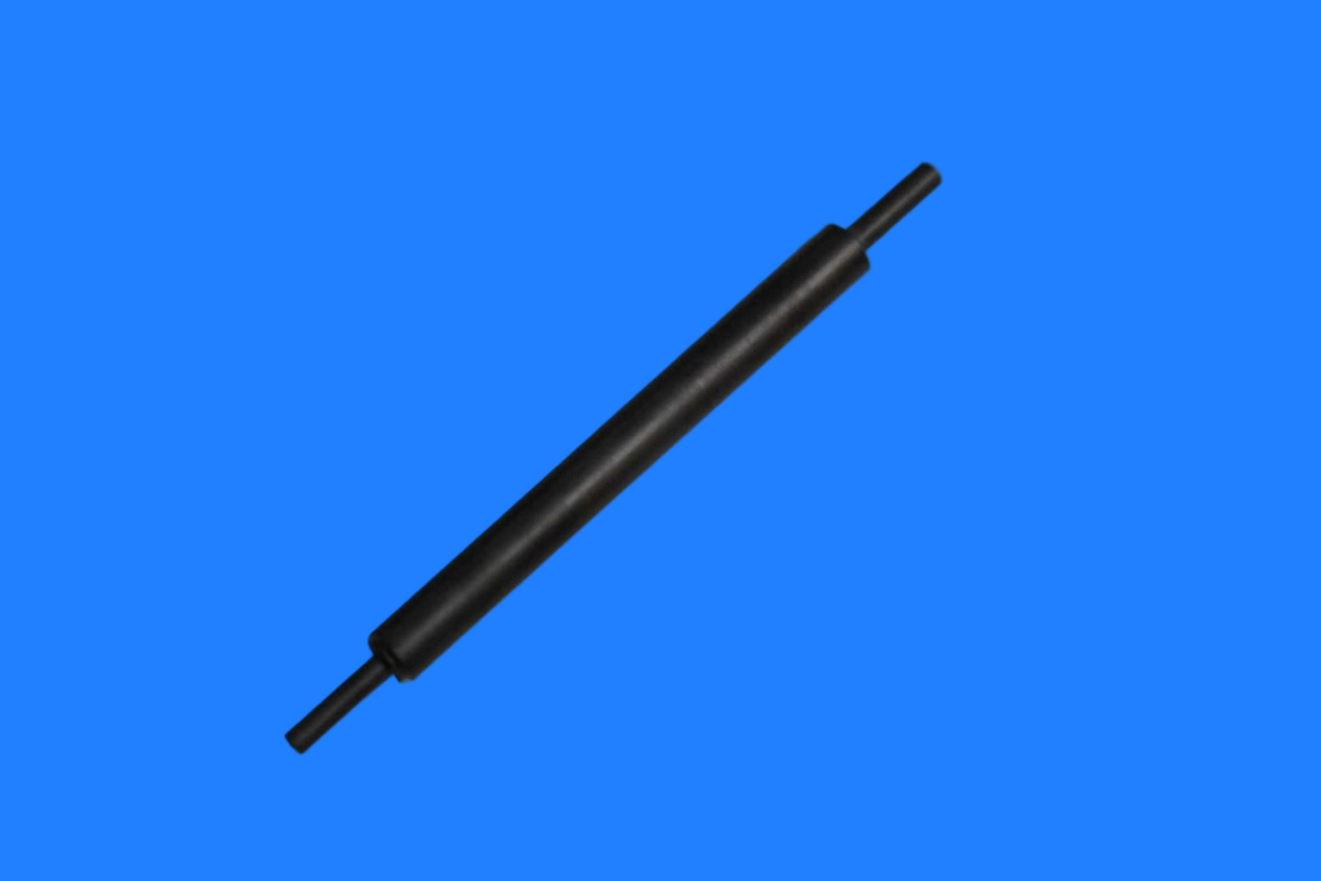
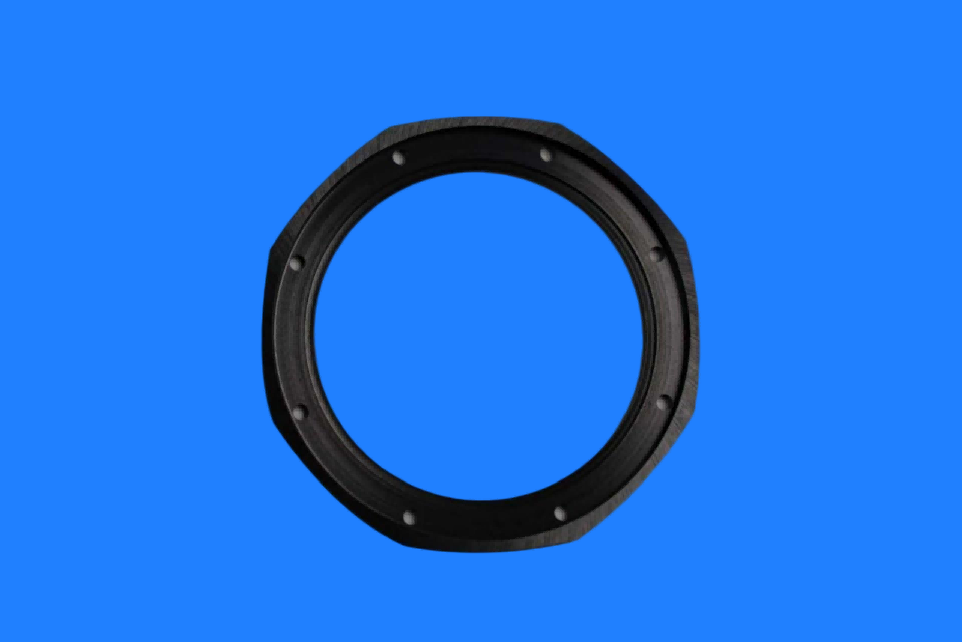
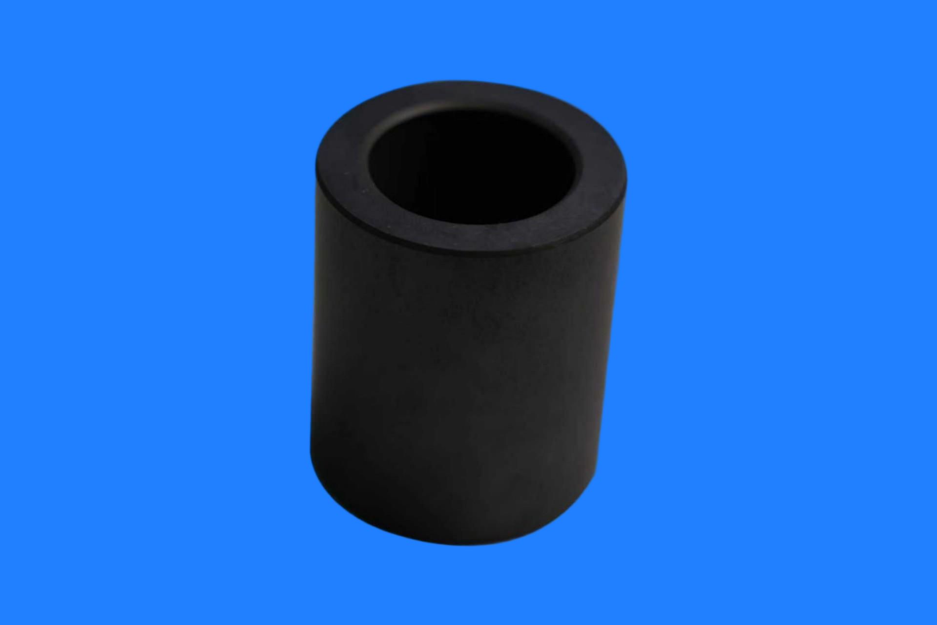
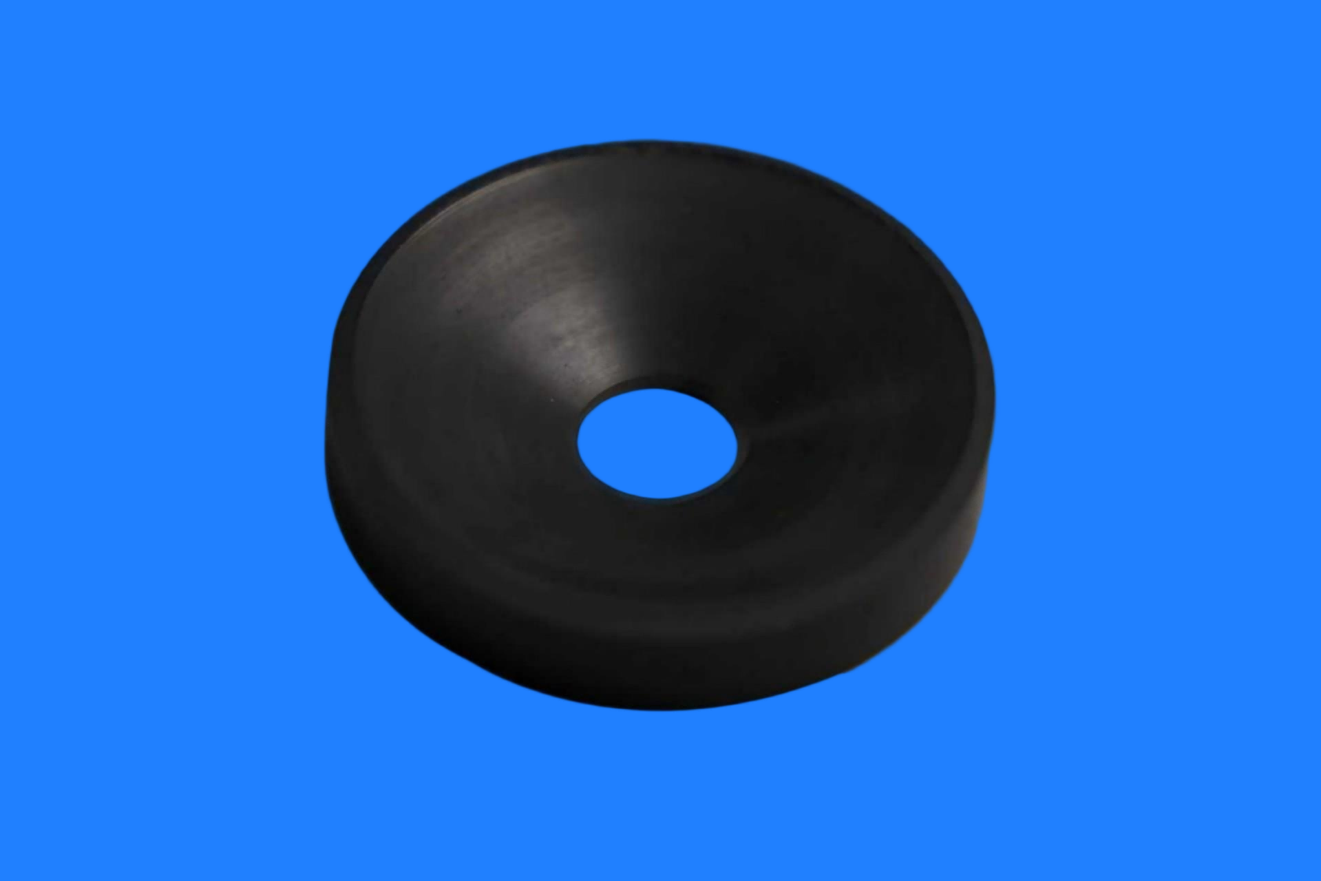
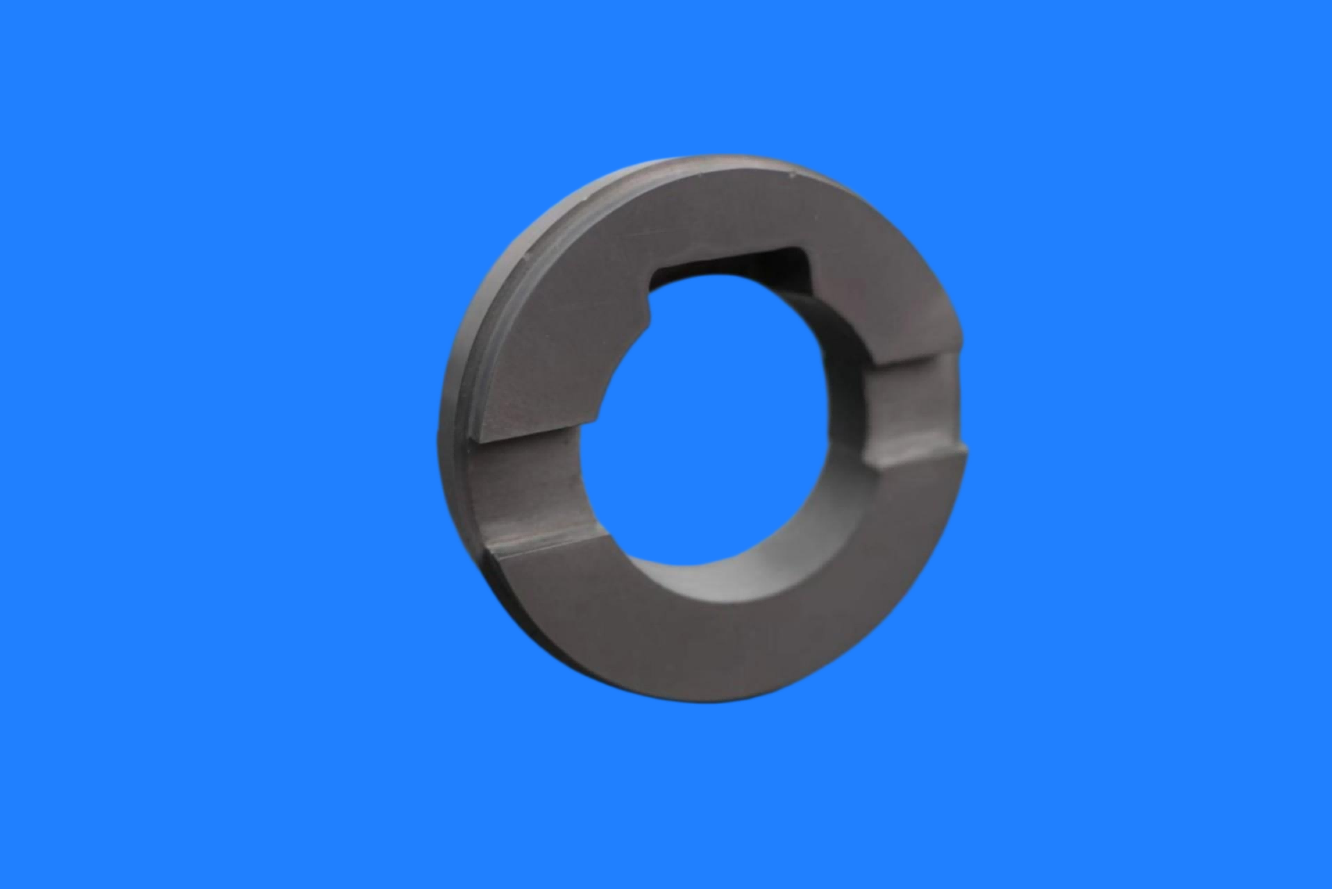
High Thermal Conductivity Silicon Carbide Ceramic Nozzle for Semiconductor Packaging
High Thermal Conductivity Silicon carbide nozzle is high-rigidity, ultra-wear-resistant, thermally stable, and extremely clean precision ceramic components, specifically designed for high-speed, high-precision, and non-destructive chip pick-and-place operations in semiconductor and microelectronics manufacturing. They are a key guarantee for achieving precision and reliability in automated production.
High Thermal Conductivity Silicon Carbide SiC Ceramic Nozzle
Product Description
Silicon carbide SiC nozzle is precision adsorption components made primarily of high-performance silicon carbide (SiC) ceramic material, belonging to the category of advanced ceramic nozzles. Compared to traditional metal or ordinary ceramic nozzles, SiC nozzles exhibit irreplaceable advantages in high-end fields such as semiconductor packaging and testing, and precision electronics manufacturing due to their inherent material properties. This product is formed through atmospheric pressure sintering or reaction sintering processes, enabling the fabrication of precision adsorption holes with a minimum diameter of 0.1 mm, meeting the manipulation requirements of micro- and nano-scale components.
Core advantages:
Key Manufacturing Processes
1.Powder Preparation: High-purity α-SiC micro powder (purity ≥99.5%, particle size 0.5-5μm) is used.
2.Forming Process: Blanks are obtained through isostatic pressing or injection molding.
3.Precision Machining: Turning, milling, and drilling are performed using diamond tools, with drilling speed controlled at 600-900 r/min.
4.High-Temperature Sintering: Sintering is carried out in an inert atmosphere at 2100-2200℃ for 2-4 hours.
5.Precision Grinding: Multi-pass precision polishing is performed using diamond polishing paste.
6.Quality Inspection: Full-dimensional inspection is performed using a coordinate measuring machine and metallographic microscope.
Typical technical parameters
| Parameters | Indicator value |
| Material density | 3.10-3.15 g/cm³ |
| Compressive strength | ≥2500 MPa |
| Elastic modulus | 410-430 GPa |
| Thermal conductivity | 120-150 W/(m·K) |
| Operating temperature | -50~1650℃ |
| Adsorption pore size | φ0.1-φ5.0mm(Customizable) |
| Flatness | ≤0.002mm |
| Parallelism | ≤0.005mm |
FAQ
Q1: What products does your company offer?
We specialize in high-performance ceramics such as alumina and silicon nitride, providing insulators, structural components, wear-resistant parts, and customized solutions.
Q2: Can you customize non-standard parts?
Yes. We support processing based on provided drawings and collaborative technical development, offering a full-process service from design to mass production.
Q3: What about accuracy and delivery time?
Standard tolerance ±0.05mm, precision grade ±0.01mm; samples 7-15 days, bulk orders 20-30 days.
Q4: Main application areas?
Power, electronics, machinery, chemical, and aerospace industries.
Q5: Quality assurance measures?
Full-process quality inspection, providing material reports and performance test data, supporting third-party certification and testing.
Q6: Do you provide technical support?
We provide professional support such as material selection consultation, design optimization, and failure analysis.
Why choose us?
1.Customized R&D, rather than standard product adaptation
2.Deep control of materials science:Material Selection Based on Needs,Microstructure Optimization,Batch Consistency
3.Precision machining capability:Flatness can reach 0.001mm, parallelism 0.002mm, and roughness Ra 0.1μm.
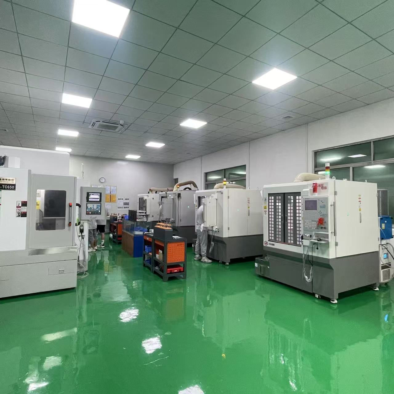
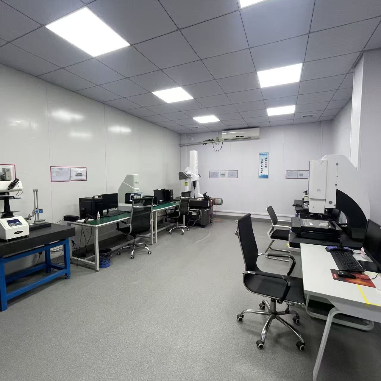
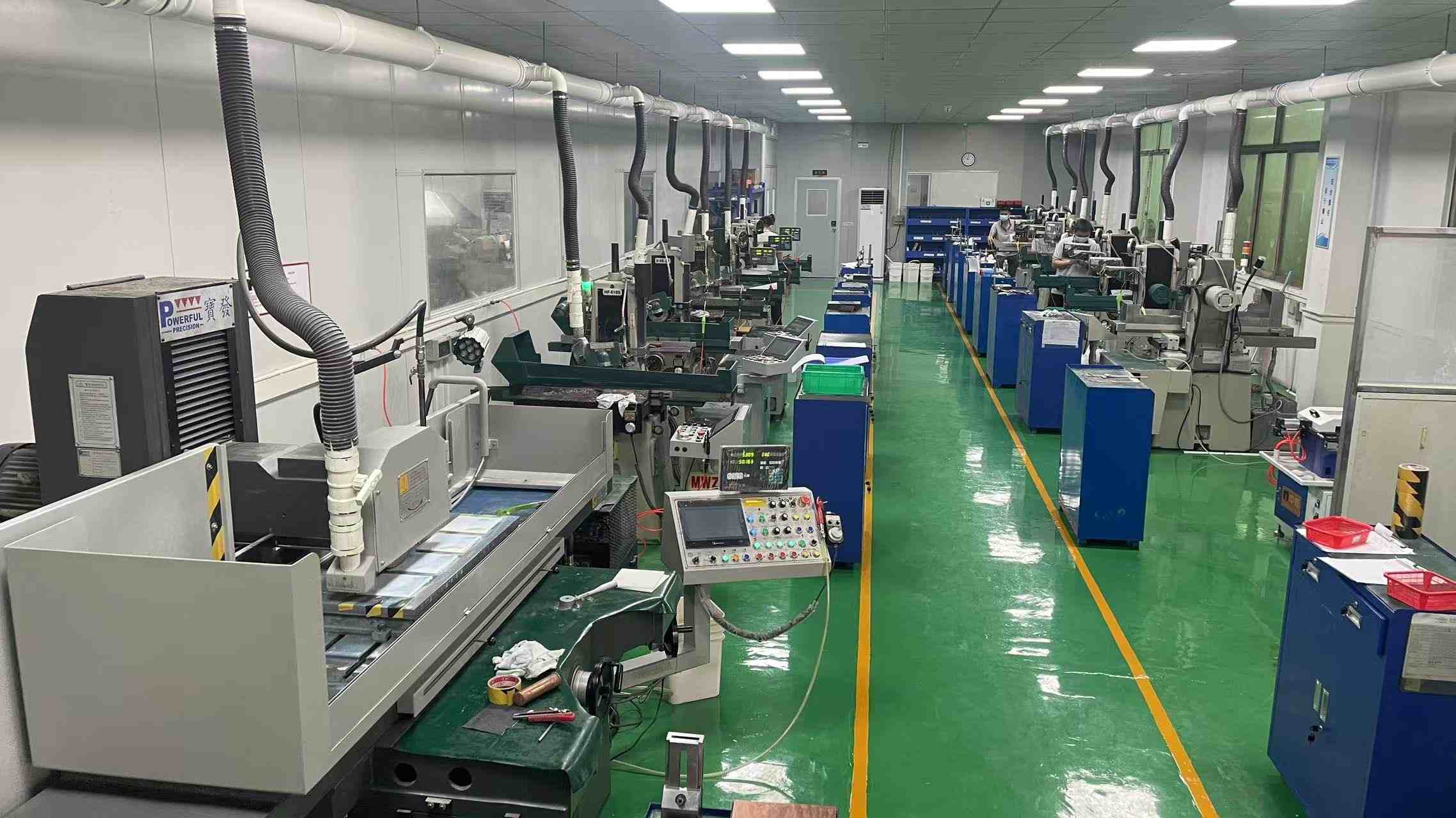
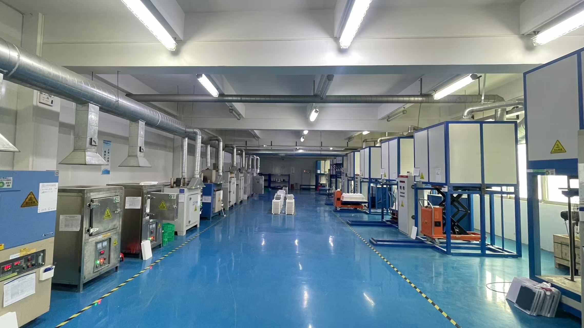
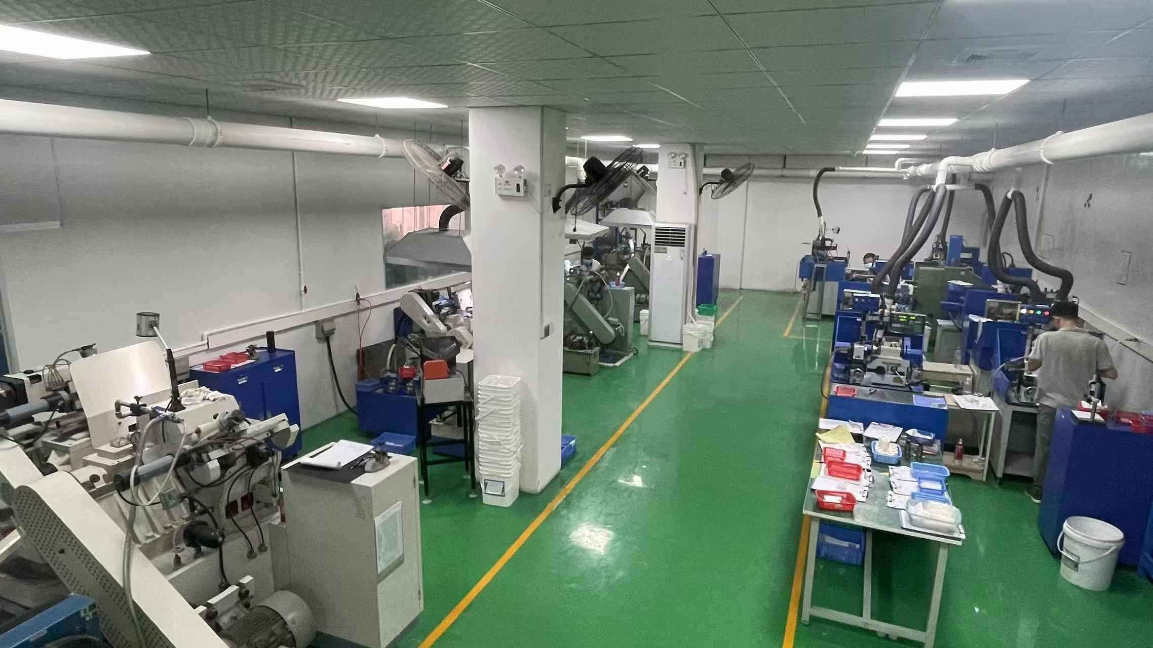
Our workshop
|
CNC Workshop |
Testing Room |
|
Surface grinding Workshop |
Sintering Workshop |
|
Circular Grinding Workshop |
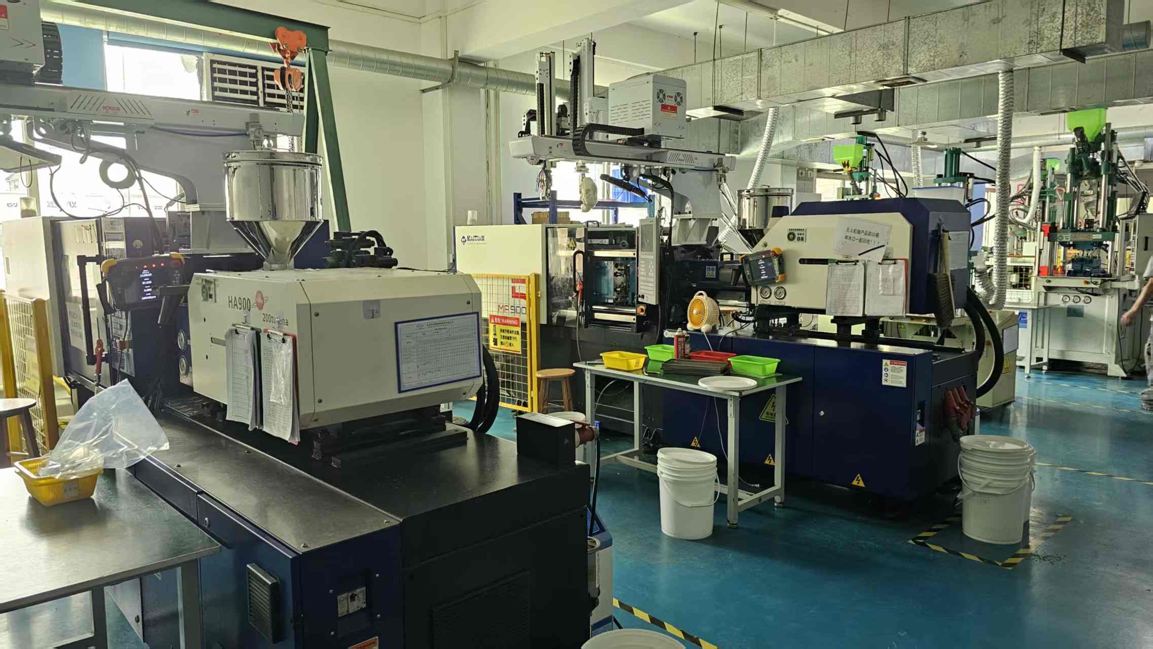
Injection molding Machine Workshop |


 IPv6 network supported
Leave A Message
Scan to Wechat :

Scan to WhatsApp :