Leave A Message
If you are interested in our products and want to know more details,please leave a message here,we will reply you as soon as we can.


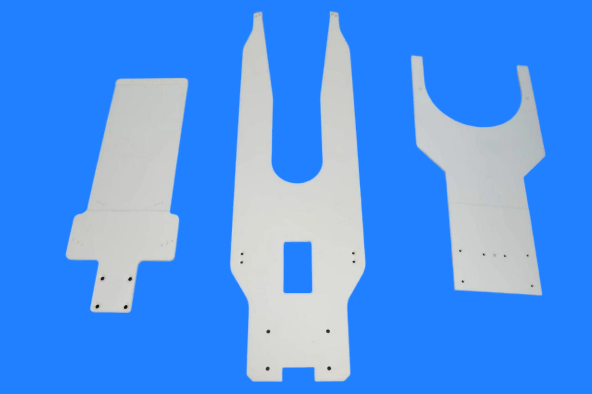
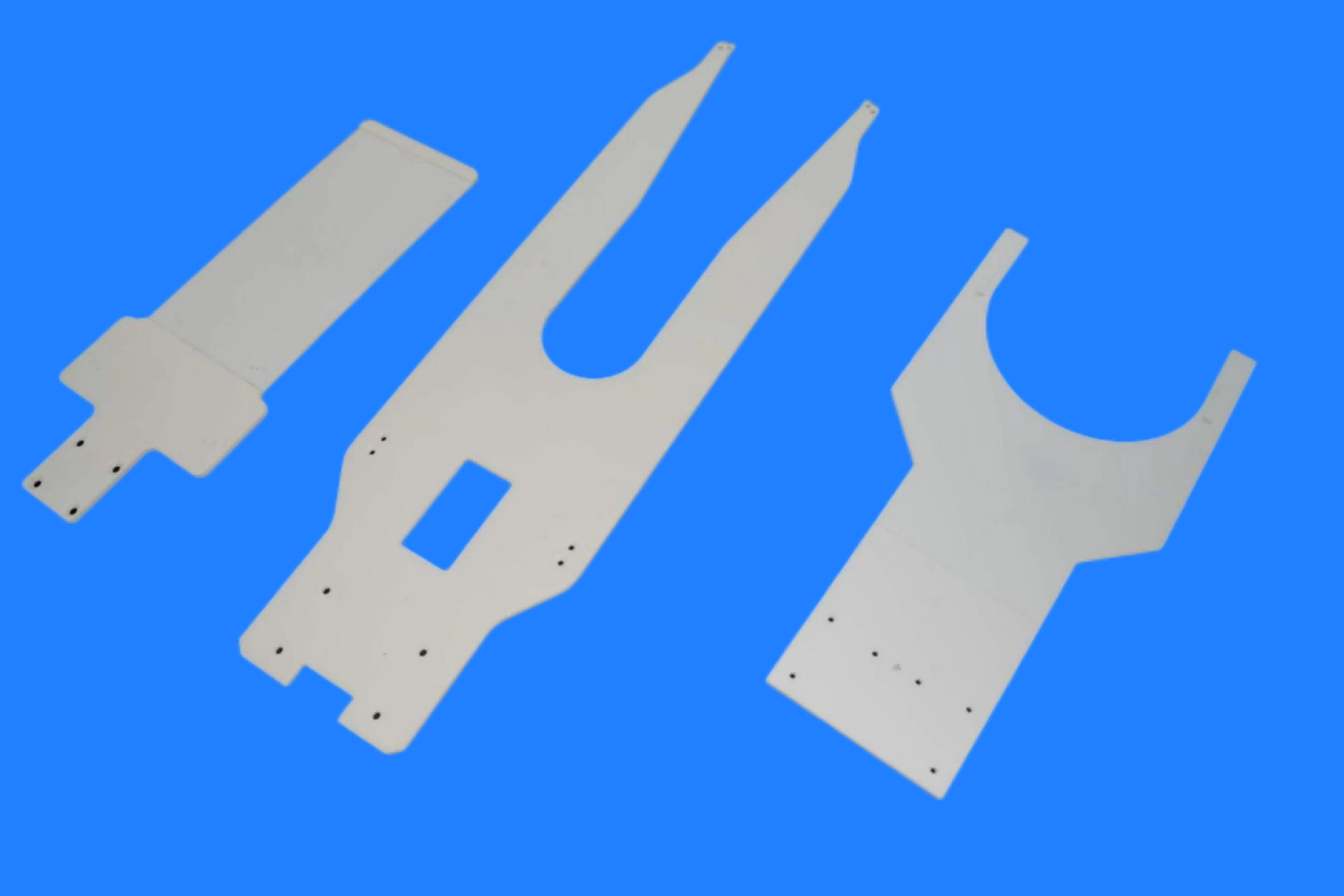
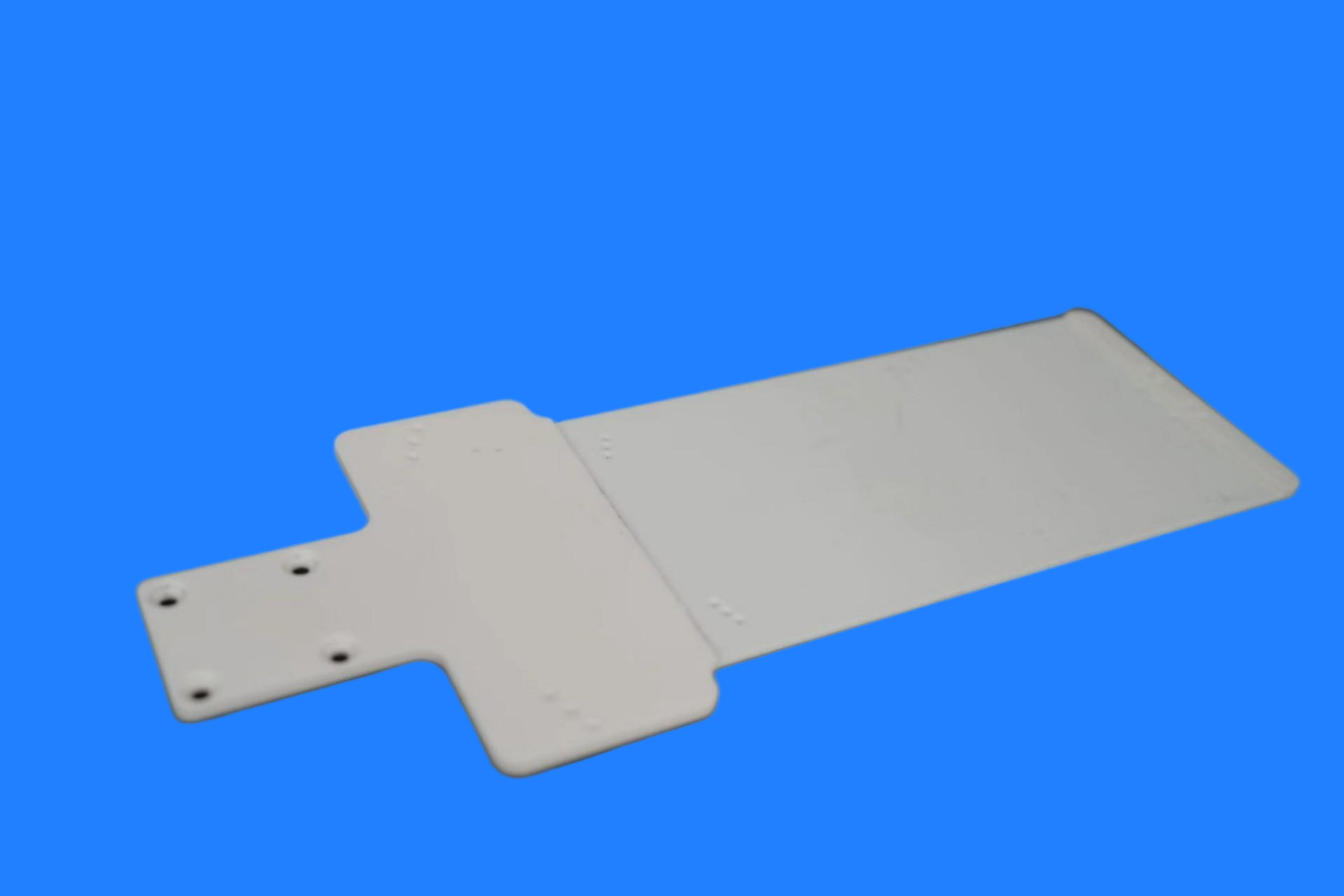
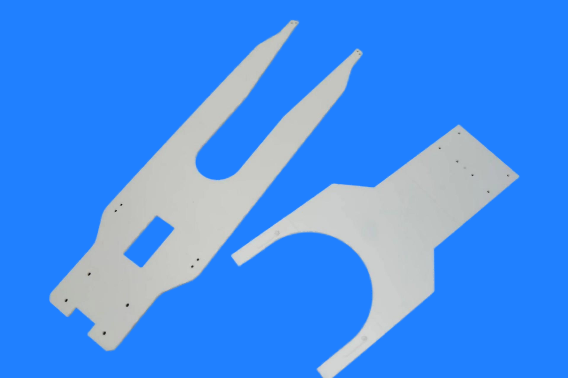
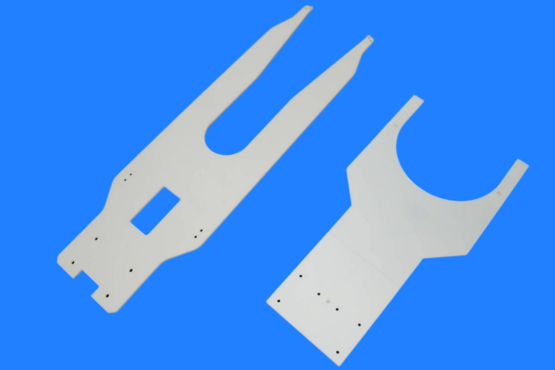
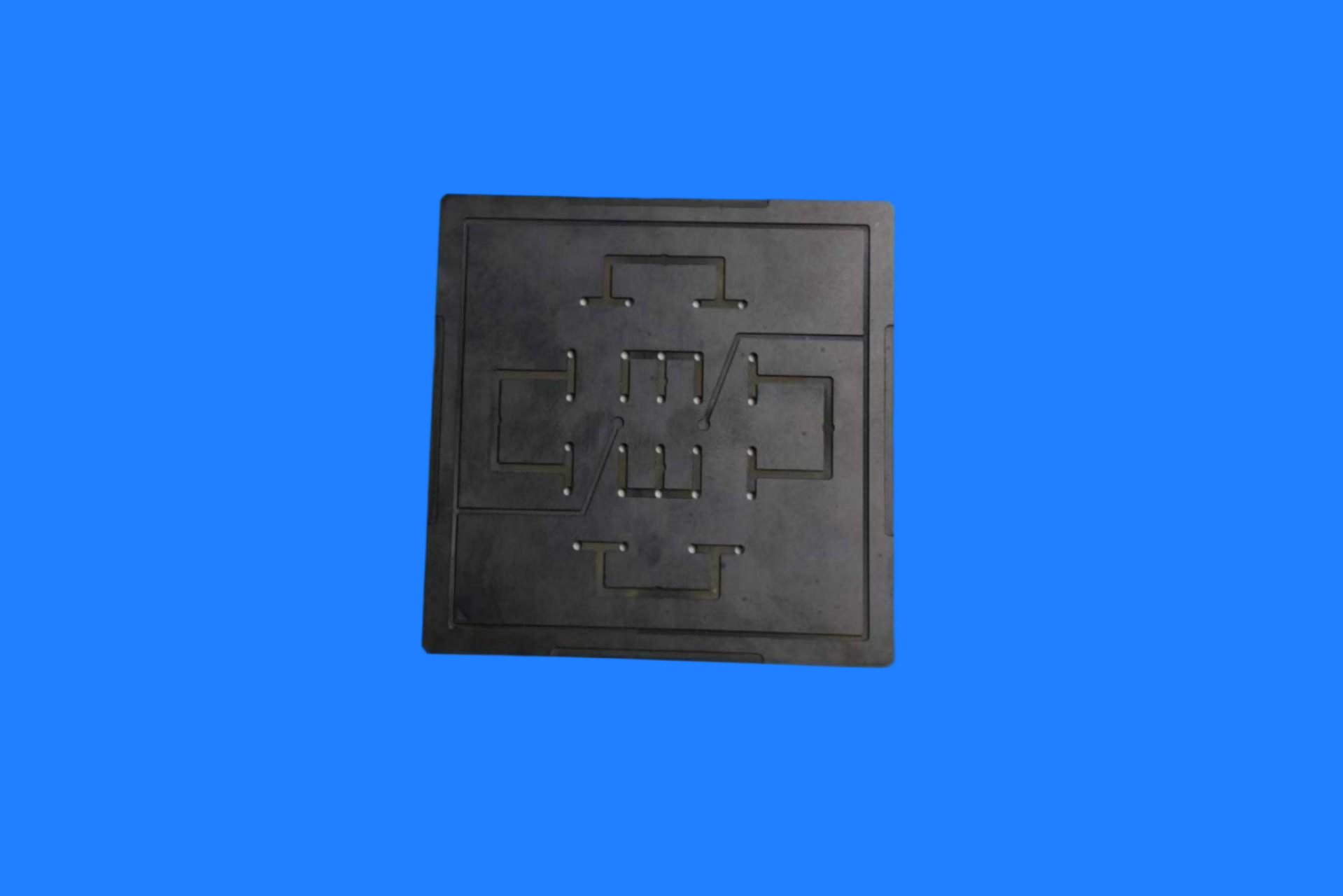
Alumina and zirconia Wafer Robot Arm is the core skeleton of high-end automated equipment, enabling high-speed, precise, and clean operation. Through the inherent superior properties of the material—lightweight, strong, stable, and clean—it solves the extreme requirements of industrial robots in cutting-edge fields such as semiconductors and electronics for speed, precision, and environmental compatibility, serving as the "precision joint" of modern intelligent manufacturing.
Al2O3 ZrO2 Wafer Robot Arm for Semiconductor
Product Positioning
High-performance Ceramic Wafer Robot Arm designed for precision transmission of 300mm/450mm wafers and wafer carriers/trays. Made of high-purity alumina (Al₂O₃) material of over 99.5%, it is suitable for wafer pick-and-place and positioning transmission in EFEM (Equipment Front-End Module), Vacuum Transfer Chamber, and high-temperature process equipment.
Core Technological Advantages
1.Ultimate Cleanliness and Zero Metal Contamination Control
(1)Material Purity: 99.5%-99.8% high-purity alumina is used, with metal impurity content <50ppm, ensuring no precipitation of metal ions such as Fe, Cu, and Na.
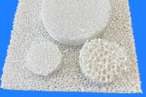
(2)Surface Characteristics: Mirror polished to Ra≤0.1μm, with no porous structure, eliminating particle shedding.
(3)Vacuum Compatibility: Vacuum bakeout treatment ensures a total mass loss (TML) <0.1%, meeting Class 1 cleanroom and high vacuum environment (<10⁻⁶ Pa) requirements.
2.Electrostatic Discharge (ESD) Control – Wafer-Level Protection
(1)Electrostatic Dissipation Design: Optional integral sintered electrostatic dissipative ceramic (uncoated), with surface resistivity precisely controlled at 10⁶–10⁹ Ω/sq.
(2)Electrostatic Pressure Control: Surface electrostatic potential <50V after friction testing, effectively preventing electrostatic discharge damage (ESD) to nanoscale circuits. Damage)
(3)No coating peeling risk: One-piece molded antistatic structure avoids particle contamination caused by peeling of traditional conductive coatings during use.
3.Micron-level precision transmission accuracy
(1)Geometric accuracy: Flatness ≤0.005mm, parallelism ≤0.003mm, ensuring repeatability of wafer positioning during photolithography and alignment processes.
(2)Thermal stability: Coefficient of thermal expansion (CTE) ~7×10⁻⁶/K, excellent thermal matching with silicon wafers (2.6×10⁻⁶/K), maintaining dimensional stability within the 100-300°C process temperature range.
(3)Lightweight and high rigidity: Density only 3.8g/cm³, 35% lighter than aluminum alloy, elastic modulus ~300GPa, achieving zero-jitter transmission under high acceleration (>3g) of robotic arms.
4.Multifunctional vacuum adsorption system
(1)Long-lasting Vacuum Holding: The precision-designed vacuum groove structure can maintain pressures of -85kPa to -80kPa for over 60 seconds and -80kPa to -25kPa for over 35 seconds during a vacuum self-holding test, ensuring wafer safety in the event of a sudden gas interruption.
(2)Low Contact Damage: The vacuum adsorption groove, combined with a Bernoulli suspension design, results in contact stress <0.1MPa, suitable for the safe handling of thin wafers (<100μm) and warped wafers.
Product lines and customization options
| Product Type | Technical features | Applicable Scenarios |
| Vacuum Suction Type | Porous ceramic/vacuum tank adsorption, supporting 4-12 inch wafers | EFEM wafer loading, Loadlock transfer, CMP equipment loading and unloading |
| Bernoulli Type | Utilizing the principle of airflow suspension, the gap between the wafer and the arm is 0.1-0.3mm. | Sensitive film wafers, back-side no-contact processes, ultra-thin wafers (<50μm) |
| Edge Grip Type | Mechanically clamps the wafer edge, achieving zero contact between the front and back sides. | Double-sided lithography and measurement equipment |
| Tray-Integrated Type | Integrated Wafer Tray carrier, supporting batch transfer of multiple wafers. | Batch Process Equipment, Annealing Process |
| High-Temp Grade | It can withstand instantaneous temperatures above 600°C and is used in hot transport. | CVD, PVD, and RTP (Rapid Thermal Processing) equipment |
Key Application Scenarios
1.EFEM and Wafer Loading SystemsTransfer
(1)300mm/450mm wafers between FOUP (Front-Opening Wafer Container) and process equipment.
(2)Matches thermal expansion with silicon wafers, avoiding positioning drift caused by temperature cycling.
2.High-Temperature Process Chamber Transfer:
(1)CVD/PVD Equipment: Withstands high-temperature process environments (>300°C), with no thermal deformation or outgassing.
(2)Diffusion Furnace: Performs wafer loading and unloading in high-temperature zones above 1000°C, replacing metal arms to avoid heat conduction contamination.
3.Cleaning and Wet Bench Processes
(1)Resistant to strong acids (HF, HCl) and strong alkalis (KOH, NH₄OH) corrosion, suitable for drying transfer after wafer cleaning and etching (Marangoni Dryer).
4. Advanced Packaging and Testing
(1)Thinned Wafer Handling: Prevents wafer breakage using Bernoulli's principle.
(2)ESD Sensitive Devices Devices Treatment: Dissipative Ceramic Protection to Prevent Device Damage
Technical Specifications
| Performance indicators | Specifications |
| Material | High-purity alumina (Al₂O₃ ≥99.5%), with optional antistatic doped type. |
| Applicable wafer size | 4 inches (100mm) to 12 inches (300mm), with 450mm custom sizes available. |
| Flatness | ≤0.005mm (critical adsorption surface) |
| Surface roughness | Ra≤0.1μm (mirror grade), Ra≤0.02μm super mirror grade is optional. |
| Surface resistivity | Insulating type: >10¹⁴ Ω·cm; Static dissipative type: 10⁶–10⁹ Ω/sq |
| Vacuum retention capability | Hold time >60 seconds at -85 kPa (standard test) |
| Temperature range | Long-term operating temperature: -50°C to +350°C; Short-term peak temperature: +600°C |
| Flexural strength | ≥350 MPa |
| Metal precipitation | <1ppb (deionized water immersion test) |
| Cleanroom Class | Compliant with ISO Class 1, and validated by IPA steam cleaning and ultrasonic cleaning. |
Quality and Certification Standards
Material Certification: Provides material composition analysis reports (ICP-MS), compliant with SEMI standards.
Cleanliness Verification: Complies with SEMI F57 (High-purity fluid systems) and SEMI E78 (Electrostatic control) specifications.
Size Standards: Follows SEMI M1 (Wafer Dimensions) and SEMI E1.9 (Mechanical Interfaces) standards.
Quality Management System: ISO 9001 certified, supports semiconductor industry PPAP (Production Part Approval Process).
Customized Services
We offer end-to-end customization from material selection, fluid dynamics simulation, precision machining to cleanroom cleaning:(1)Vacuum Loop Design: Optimize pore size and channel layout based on the customer's vacuum source pressure to ensure uniform adsorption.(2)ESD Protection Customization: Precisely adjust surface resistivity (10⁴–10¹¹ Ω range) to match specific process electrostatic safety requirements.(3)Lightweight Structure: Reduce weight by 20-30% while maintaining rigidity through topology optimization and cavity structure design.(4)Marking and Traceability: Support laser marking or mechanical engraving to meet the traceability requirements of semiconductor components.


 IPv6 network supported
Leave A Message
Scan to Wechat :

Scan to WhatsApp :