Leave A Message
If you are interested in our products and want to know more details,please leave a message here,we will reply you as soon as we can.


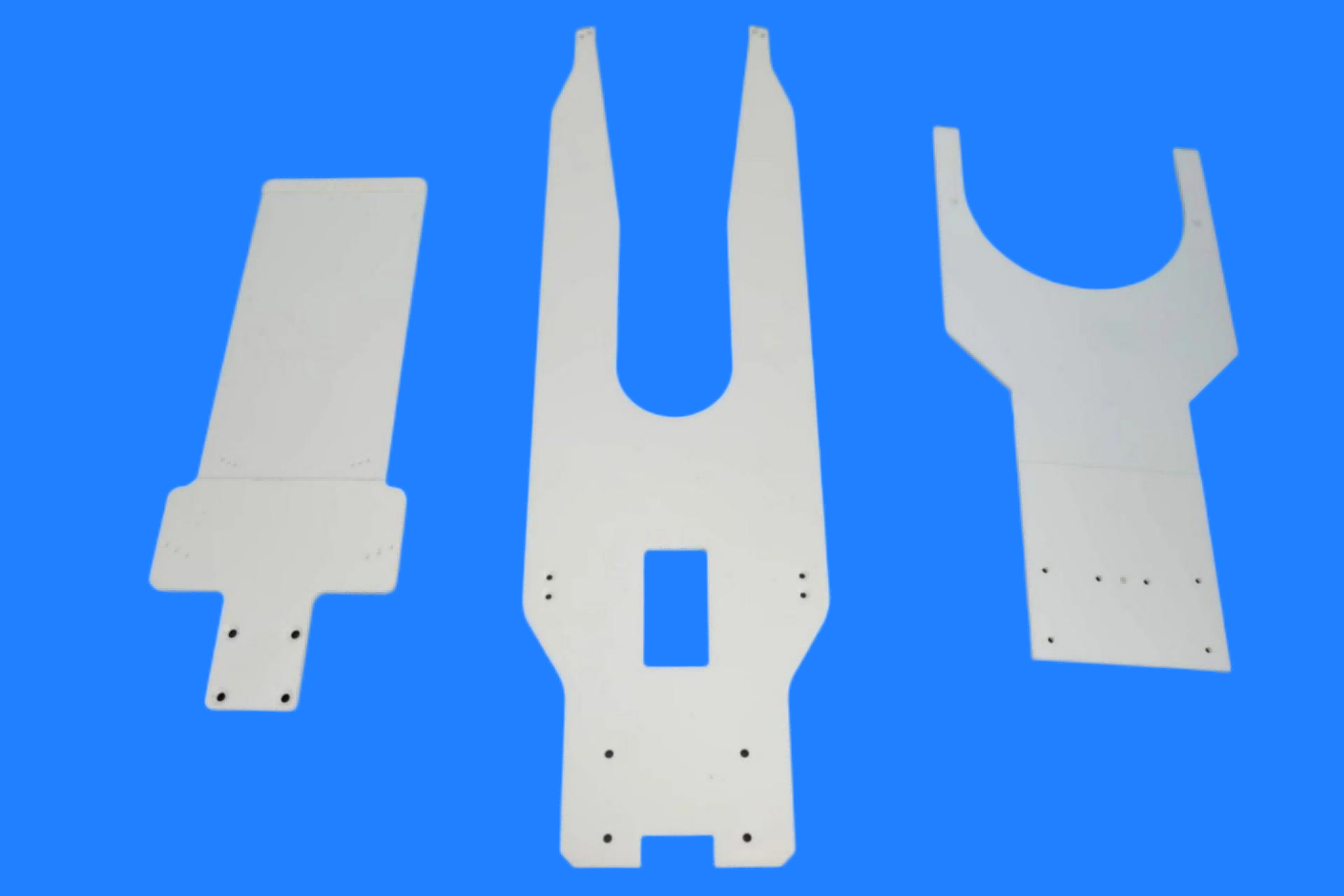
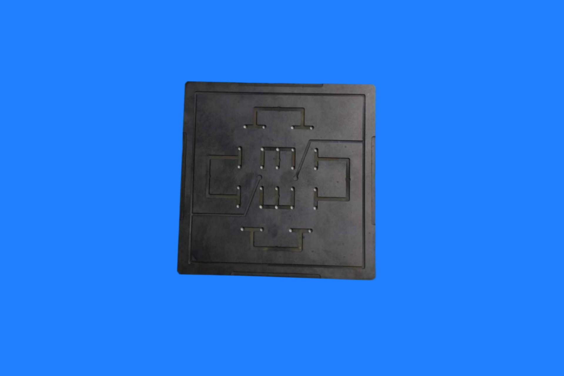
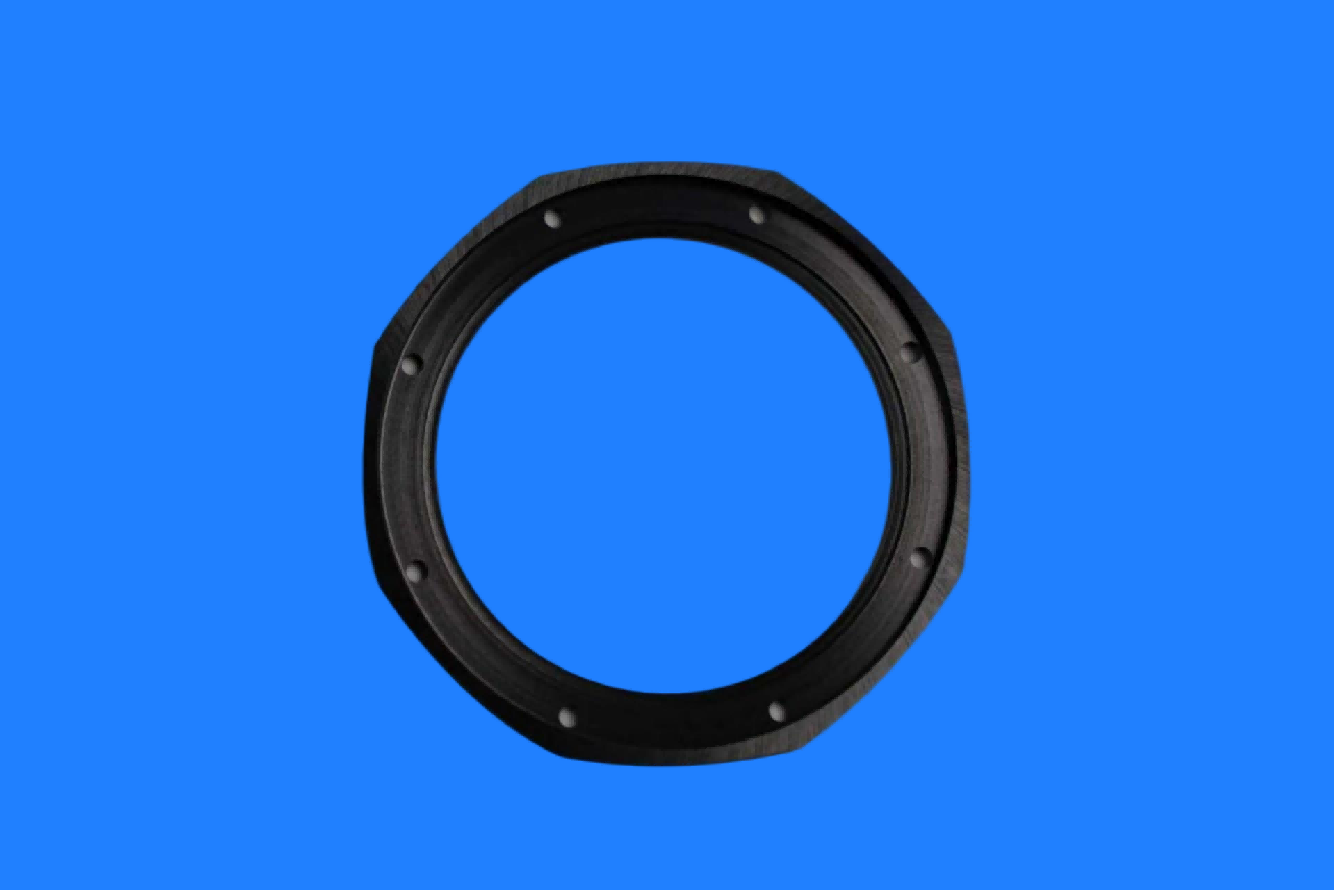
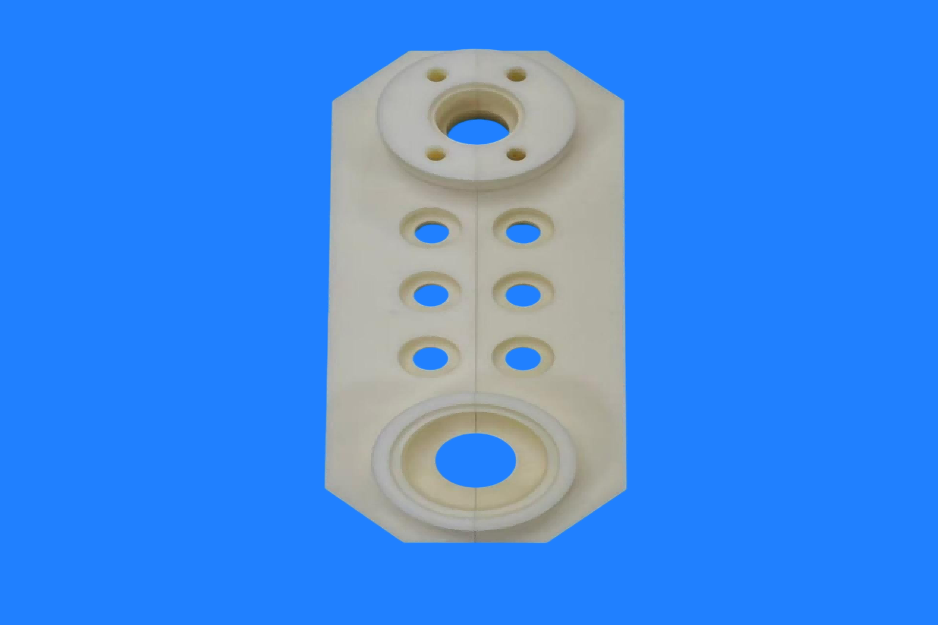
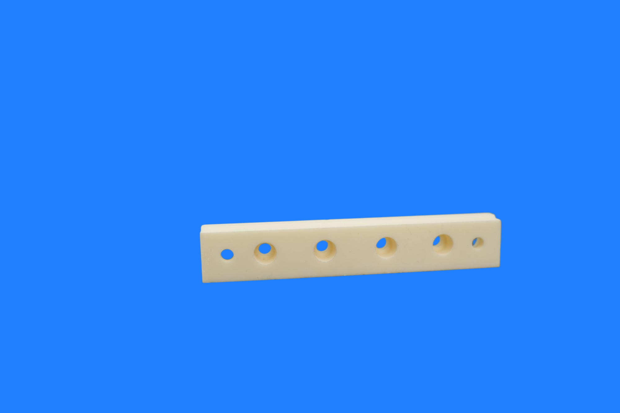
99.9% High Purity Alumina Ceramic Distributor Plate for PECVD, LPCVD, and MOCVD
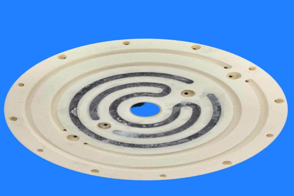
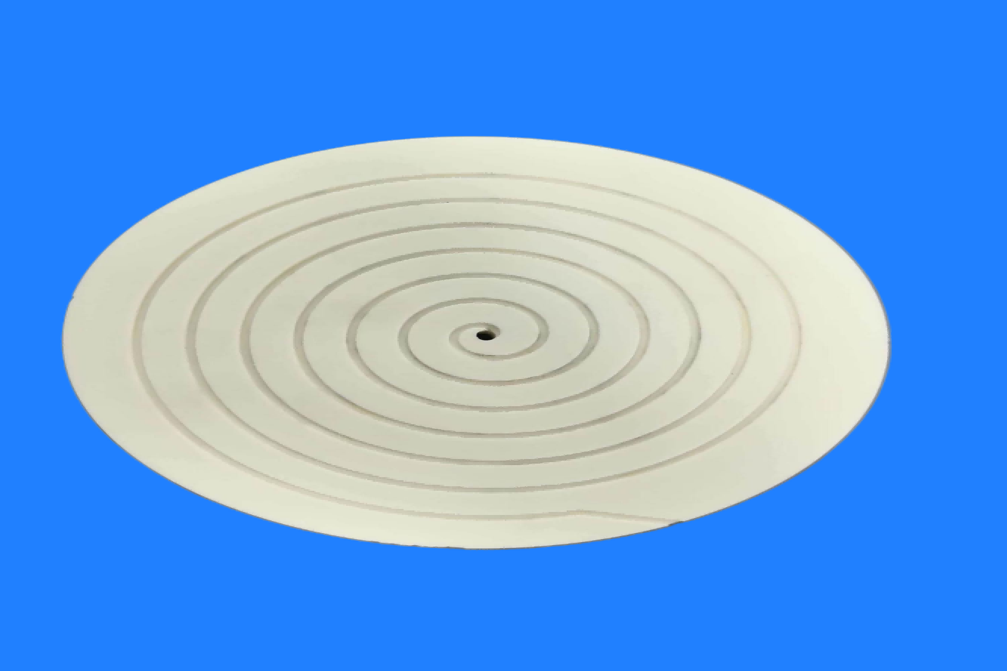
The 99.9% Alumina Ceramic Distribution Plate is a critical precision component for semiconductor etching, CVD, and ALD thin-film deposition equipment. It is widely used in key process steps such as Chemical Vapor Deposition (CVD), Atomic Layer Deposition (ALD), Physical Vapor Deposition (PVD), and plasma etching. Featuring a design that combines spiral concentric flow channels with a multi-layer gas buffering structure, the plate uniformly disperses plasma and process gases, ensuring processing consistency across the entire wafer.
99.9% High Purity Alumina Ceramic Distributor Plate for PECVD, LPCVD, and MOCVD
Product Description
The primary function of this High-purity Al₂O₃ Ceramic Gas Distribution Plate is to distribute process gases evenly and stably onto the wafer surface, thereby ensuring uniform thin-film deposition thickness, etching precision, and process repeatability. Its performance directly determines the uniformity of thin films, etching accuracy, and process yields during wafer fabrication. Manufactured from high-purity alumina (Al₂O₃) ceramic material (purity ≥99.9%) using precision forming, high-temperature sintering, and ultra-precision micro-hole machining technologies, the product offers significant advantages—including high chemical stability, excellent corrosion resistance, high electrical insulation, and low particle generation—making it an ideal replacement for traditional metal gas distribution plates.
Key Material Properties
99.9% high-purity alumina ceramic (also known as 3N-grade alumina) is one of the preferred materials for semiconductor equipment components, offering the following outstanding properties:
| Performance Indicators | Typical Values | Functional Significance |
| Purity | ≥99.9%(Al₂O₃) | ultra-low impurity content to prevent metal contamination of wafers. |
| Density | 3.9–3.94 g/cm³ | dense structure, free of voids, preventing gas permeation and leakage. |
| Vickers Hardness | 18–20 GPa (approx. 2000 HV) | high wear resistance, extending service life. |
| Flexural Strength | 330–400 MPa | high mechanical strength; withstands installation and process stresses. |
| Modulus of Elasticity | 390–393 GPa | high rigidity; maintains dimensional stability. |
| Thermal Conductivity | 27–32 W/(m·K) | rapid temperature equalization; stabilizes the process temperature field. |
| Coefficient of Thermal Expansion | 8.0×10⁻⁶ /K | matches the thermal expansion of silicon wafers, reducing thermal stress. |
| Maximum Operating Temperature | 1700°C | compatible with high-temperature deposition and annealing processes. |
| Volume Resistivity | >10¹⁴ Ω·cm(20°C) | excellent electrical insulation properties; prevents electrostatic damage. |
| Dielectric Constant | ≈9.7 | suitable for high-frequency plasma environments. |
| Dielectric Loss | <3.0×10⁻⁴ | low dielectric loss ensures RF transmission efficiency. |
| Dielectric Strength | >15 kV/mm | high resistance to dielectric breakdown |
Product Structure and Functional Principles
1. Core Functions
The core function of the showerhead is to transform concentrated incoming process gases—via internal precision channels and arrays of micro-holes—into a low-turbulence, highly uniform laminar flow that is evenly distributed across the wafer surface. This achieves the following:
(1)Thin-film deposition uniformity: Ensures film thickness variation across the wafer surface is <±3%.
(2)Etching uniformity: Prevents localized over-etching or under-etching.
(3)Uniform plasma distribution: Acts as an electrode in PECVD/etching processes to generate a uniform electric field.
(4)Coordinated temperature control: Works in conjunction with the wafer susceptor to maintain stable process temperatures.
2.Typical structural composition
| Structural Module | Feature Description | Precision Requirements |
| Gas Distribution Chamber | optimizes internal airflow paths and utilizes CFD simulation to reduce pressure loss, ensuring uniform gas distribution. | runner tolerance ±0.05 mm |
| Micropore Array | densely arranged through-holes with diameters of 0.1–1.0 mm convert the gas into uniform laminar flow. | aperture tolerance ±0.01 mm |
| Sealing Surface | works in conjunction with the cavity seal to prevent gas leakage. | flatness ≤ ±2 μm |
| Surface Coating (optional) | corrosion-resistant SiC or nitride coatings deposited via PVD/CVD | coating thickness uniformity ±5% |
Key Technical Parameters
| Parameter Items | Technical Specifications |
| Purity Grade | ≥99.9% (3N grade); 99.99% (4N grade) optional |
| Grain Size | average <6 μm (dense microstructure) |
| Water Absorption Rate | 0% (fully dense sintering) |
| Gas Permeability | 0% (passed helium leak test) |
| Micropore Diameter | Φ0.2–6 mm (customized according to the process) |
| Micropore Tolerance | ±0.01 mm |
| Micro-hole Depth-to-diameter Ratio | up to 50:1 |
| Bore Wall Roughness | Ra ≤0.2 μm |
| Surface Flatness | ≤±2 μm (entire area) |
| Surface Roughness | Ra ≤0.01–0.1 μm (capable of mirror polishing) |
| Applicable Wafer Specifications | 6-inch / 8-inch / 12-inch |
| Maximum Outer Diameter | Φ300 mm and above (customizable) |
| Operating Temperature Range | ambient temperature to 1000°C |
| Corrosion-resistant Gas | F₂、Cl₂、CF₄、SF₆、HF、O₂、NH₃ and so on |
Product Core Competitive Advantages
1.Ultra-high purity, zero metal contamination
Purity ≥99.9%; impurity levels (e.g., Na, Si) <100 ppm
No metal ion leaching, preventing metal contamination of wafers
Meets stringent material purity requirements for advanced process nodes (≤7 nm)
2.Exceptional Corrosion Resistance
Highly resistant to strongly corrosive plasma gases, such as fluorine-based (F₂, CF₄, SF₆) and chlorine-based (Cl₂) gases
Dense microstructure blocks the permeation of corrosive gases, preventing internal erosion
Maintains surface integrity for extended periods in plasma etching environments and generates minimal particles
3.Precision Micro-hole Machining Technology
Utilizes a hybrid process combining laser drilling and precision grinding to achieve high-precision micro-hole machining.
Maintains a hole diameter consistency of ±0.01 mm, ensuring uniform gas flow distribution.
Capable of machining ultra-deep micro-holes with an aspect ratio of 50:1, meeting the requirements of complex airflow path designs.
4.Excellent thermal stability and insulation properties
Coefficient of thermal expansion matches that of silicon wafers, resulting in minimal deformation during temperature fluctuations
Volume resistivity >10¹⁴ Ω·cm; maintains stable electrical insulation in high-frequency plasma environments
Stable dielectric constant; suitable for RF power transmission at frequencies above 1 GHz
5.Exceptionally long service life and low maintenance costs
Vickers hardness of 18–20 GPa; wear resistance far superior to traditional materials like aluminum alloys
Service life in corrosive environments is 3–5 times that of metal flow plates
Reduces the frequency of maintenance-related downtime and improves Overall Equipment Effectiveness (OEE)
6.High-Purity Assurance
Surface polishable to a mirror finish (Ra < 0.01 μm) with minimal particle shedding
Compliant with Class 1 cleanroom standards
Fully dense, pore-free structure prevents gas entrapment and cross-contamination
Applications
1. Chemical Vapor Deposition (CVD)
In thin-film deposition equipment such as PECVD, LPCVD, and MOCVD, the gas distribution plate uniformly disperses precursor gases onto the wafer surface, enabling the high-quality deposition of SiO₂, Si₃N₄, polysilicon, and metal films (e.g., TiN, W).
2.Atomic Layer Deposition (ALD)
The ALD process places extremely high demands on gas uniformity; high-purity alumina gas distribution plates maintain structural stability at high temperatures exceeding 600°C, ensuring precise control of film thickness at the atomic layer level.
3.Plasma Etching
In dry etching equipment, the gas distribution plate—which also serves as an RF electrode—uniformly introduces etching gases (such as CF₄, Cl₂, and SF₆) into the plasma chamber while withstanding high-energy ion bombardment. High-purity alumina exhibits plasma corrosion resistance that is significantly superior to that of metallic materials.
4.Physical Vapor Deposition (PVD)
In sputtering deposition equipment, a gas distribution plate is used to evenly distribute sputtering gases (such as Ar and N₂) and maintain a stable sputtering plasma environment.
5.Advanced Packaging and Display Panel Manufacturing
In wafer-level packaging (WLP), fan-out packaging, and OLED evaporation equipment, high-purity alumina gas distribution plates are used for the precise distribution of process gases, ensuring packaging yields and uniform light emission in display panels.
Customization Capabilities
We offer comprehensive custom design and manufacturing services, tailored to specific equipment models and process requirements:
All products are manufactured, cleaned, inspected, and packaged in a Class 10 (ISO 4) cleanroom environment to ensure delivery free from particle contamination. Each batch is accompanied by comprehensive reports covering elemental analysis, dimensional inspection, and helium leak testing.
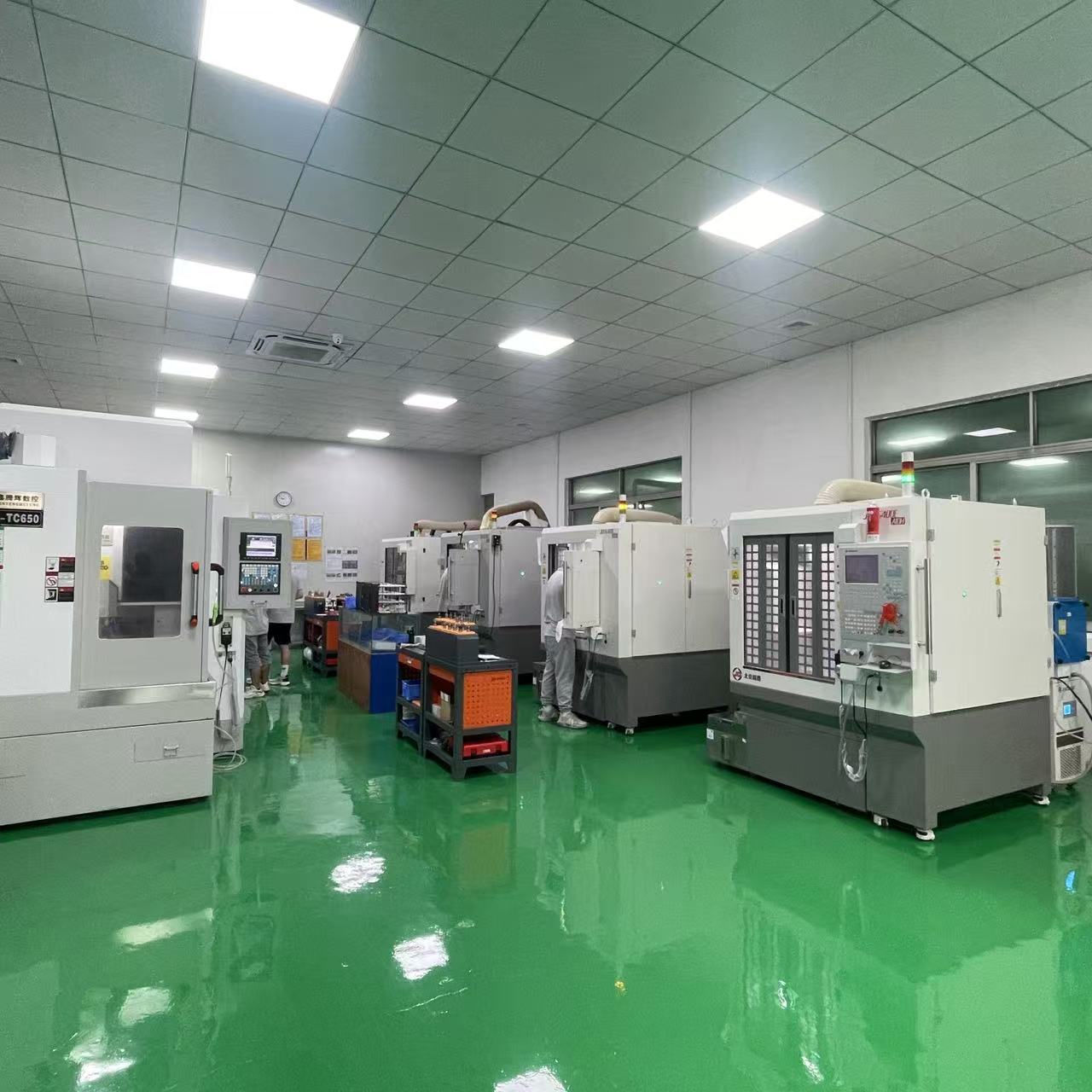
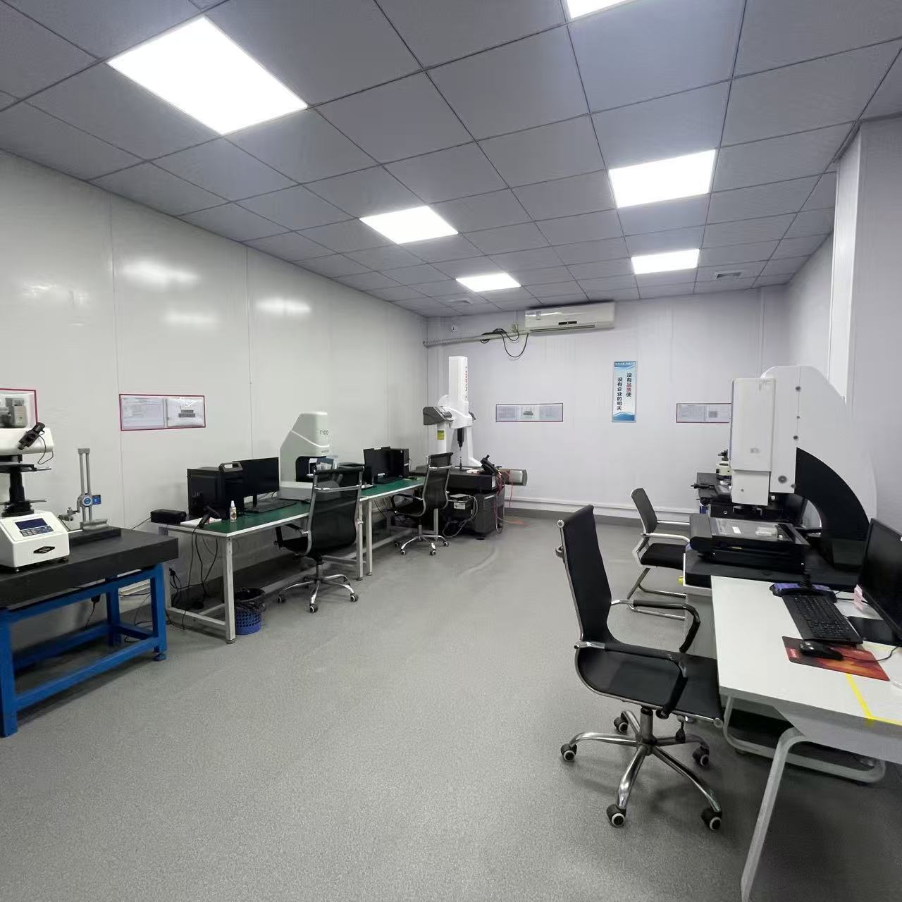
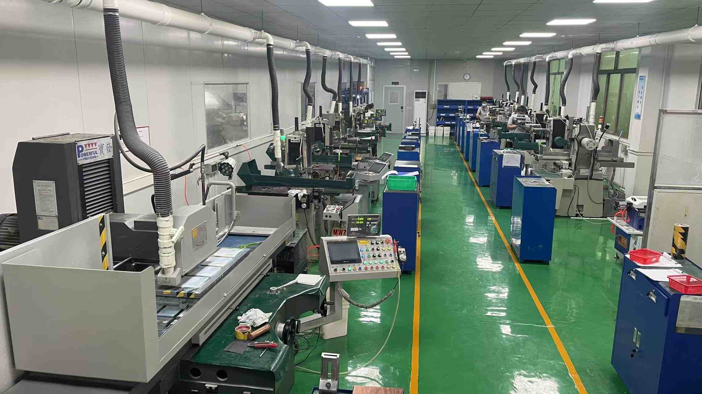
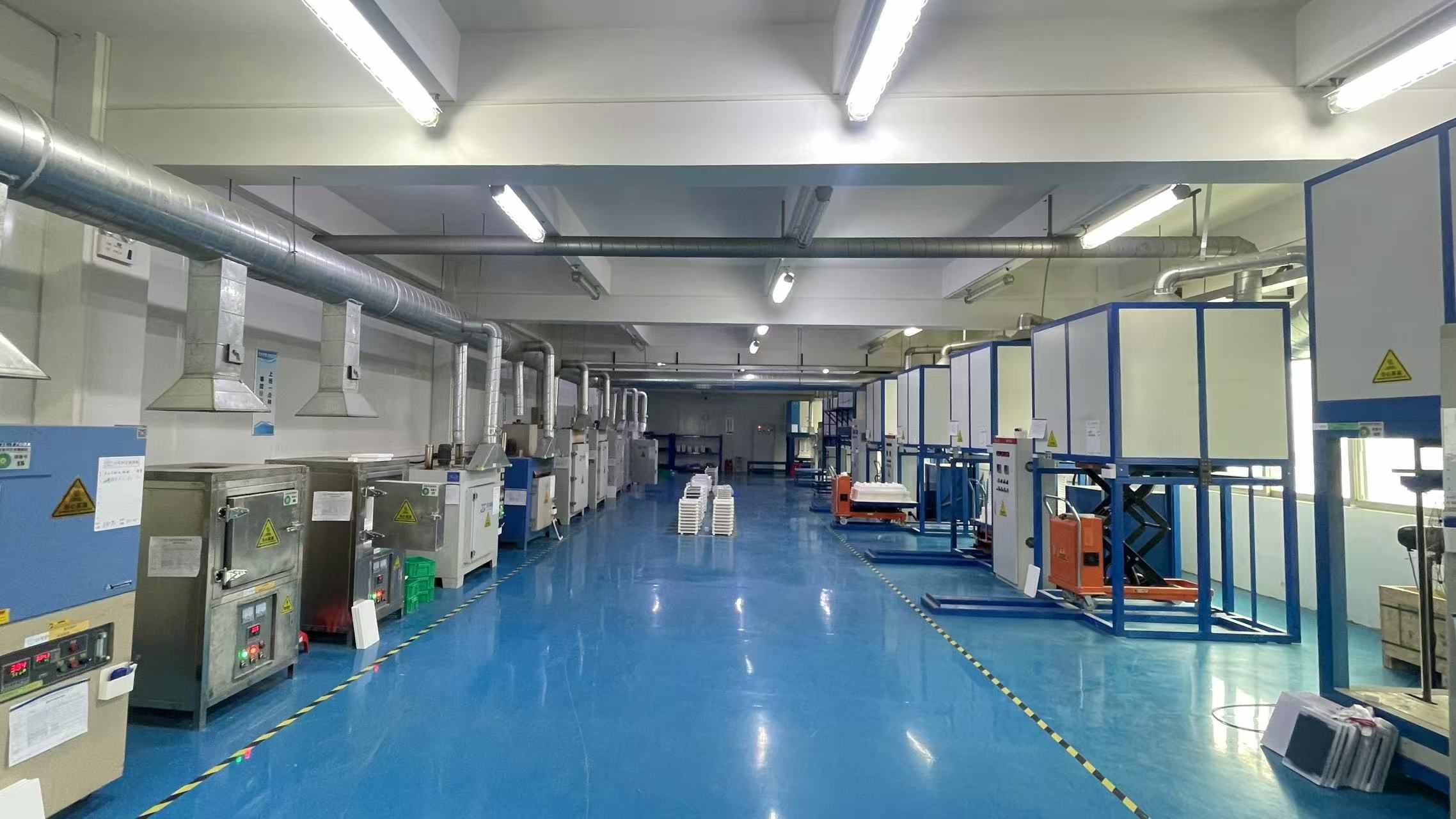
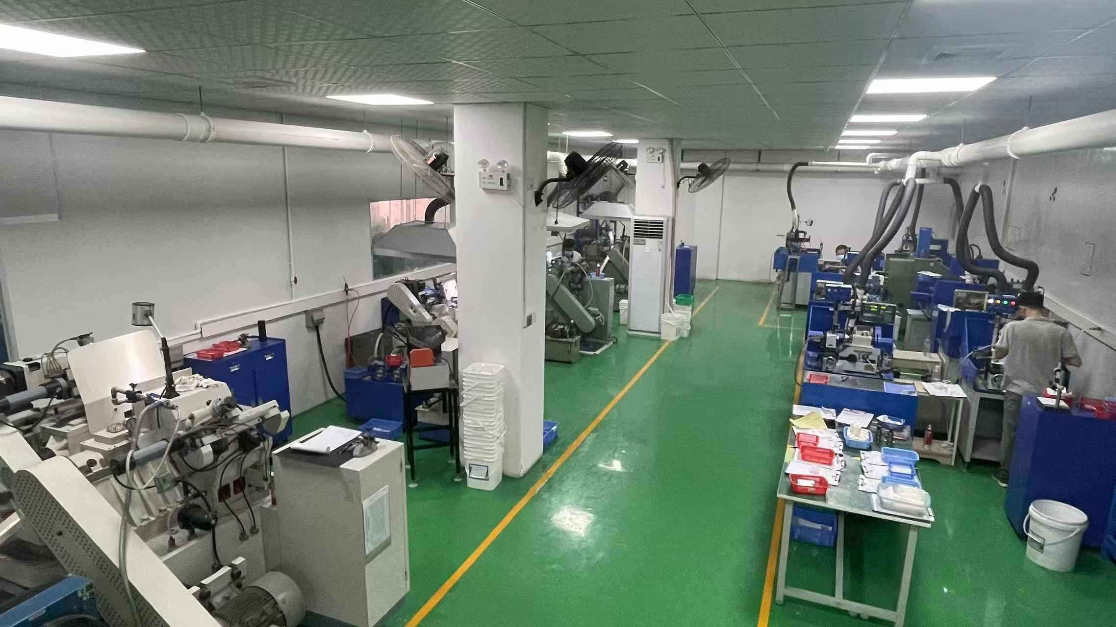
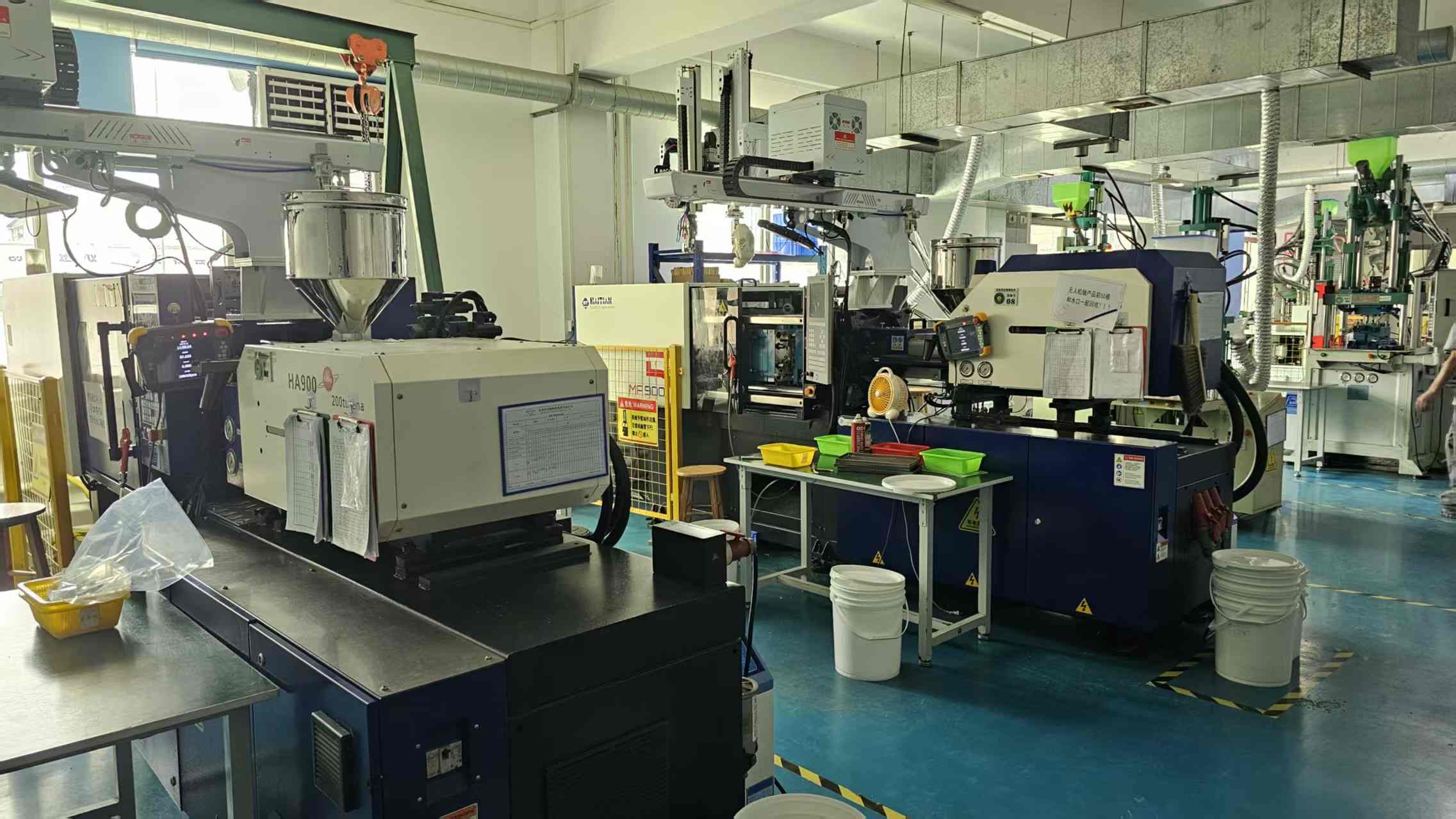
Our workshop
|
CNC Workshop |
Testing Room |
|
Surface grinding Workshop |
Sintering Workshop |
|
Circular Grinding Workshop |
Injection molding Machine Workshop |
Why choose us?
1.Customized R&D, rather than standard product adaptation
2.Deep control of materials science:Material Selection Based on Needs,Microstructure Optimization,Batch Consistency
3.Precision machining capability:Flatness can reach 0.001mm, parallelism 0.002mm, and roughness Ra 0.1μm.
FAQ
Q1: What products does your company offer?
We specialize in high-performance ceramics such as alumina and silicon nitride, providing insulators, structural components, wear-resistant parts, and customized solutions.
Q2: Can you customize non-standard parts?
Yes. We support processing based on provided drawings and collaborative technical development, offering a full-process service from design to mass production.
Q3: What about accuracy and delivery time?
Standard tolerance ±0.05mm, precision grade ±0.01mm; samples 7-15 days, bulk orders 20-30 days.
Q4: Main application areas?
Power, electronics, machinery, chemical, and aerospace industries.
Q5: Quality assurance measures?
Full-process quality inspection, providing material reports and performance test data, supporting third-party certification and testing.
Q6: Do you provide technical support?
We provide professional support such as material selection consultation, design optimization, and failure analysis.



 IPv6 network supported
Leave A Message
Scan to Wechat :

Scan to WhatsApp :