Leave A Message
If you are interested in our products and want to know more details,please leave a message here,we will reply you as soon as we can.


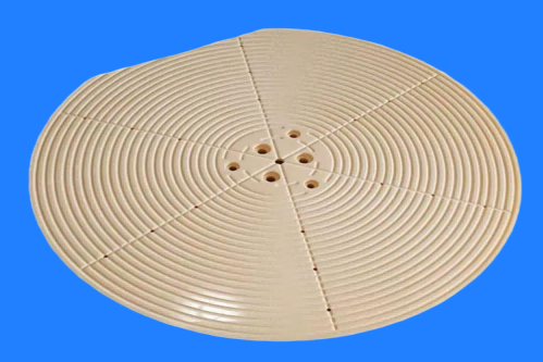
This 99.9% Alumina Vacuum Chuck is manufactured using 99.9% ultra-high-purity alumina (Al₂O₃) precision ceramic material, processed via high-temperature sintering and precision machining; it is specifically designed for the semiconductor, optoelectronics, and precision manufacturing sectors. It combines high rigidity, a low coefficient of thermal expansion, superior flatness, and a uniform microporous structure, enabling stable, non-damaging, and contamination-free vacuum clamping of precision workpieces such as wafers, silicon substrates, and glass panels.
99.9% High-Purity Porous Alumina Ceramic Vacuum Chuck
Product Description
This 99.9% High-purity Ceramic Vacuum Chuck serves as a precision vacuum-holding component for equipment used in wafer probing, optical coating, and electronic substrate processing. The chuck surface features a six-zone airflow design with concentric spiral grooves, ensuring uniform negative pressure for the stable holding of precision substrates like 4/6-inch wafers and ultra-thin glass. High-purity alumina offers exceptional electrical insulation, chemical resistance (acid/alkali), and high-temperature stability; it prevents high-voltage arcing within the chamber and eliminates impurity-induced contamination. The dense, polished surface generates minimal particulates, effectively enhancing product yield. Compared to silicon carbide or zirconia chucks, this product offers superior cost-performance in low-to-medium temperature applications free from intense plasma corrosion. Fully customizable regarding dimensions, airflow paths, and heating channels, the product undergoes vacuum leak testing and cleanroom cleaning prior to shipment, providing a one-stop alumina ceramic customization service for global semiconductor, optical, and electronics manufacturers.
Product Specifications
1. Dimensions: circular (customized); diameter 80–300 mm, thickness 5–30 mm; disk surface flatness ≤0.002 mm, parallelism ≤0.001 mm
2. Air channel groove structure
Product Core Advantages
1. Ultra-high purity and exceptional cleanliness
With an alumina purity of ≥99.9% and strictly controlled levels of impurities such as Na, Fe, and Si (Na ≤2 ppm, Fe ≤3 ppm, Si ≤10 ppm), the material effectively prevents metal ion contamination and particle defects during wafer processing, meeting the rigorous cleanliness requirements of advanced manufacturing processes.
2. Precision microporous structure for uniform suction
Utilizing porous ceramic technology, the material features a micropore size range of 2–100 μm (customizable), a porosity of 30%–50%, and an interconnected pore network. The suction force is evenly distributed, with the pressure differential controlled within ±5 kPa across a 10×10 mm area, ensuring that thin workpieces (such as silicon wafers and thin films) remain free from deformation and suction marks.
3.Ultra-high geometric precision
Flatness: ≤3 μm (4–6 inch), ≤5 μm (8 inch), ≤10 μm (12 inch)
Parallelism: ≤3 μm
Surface roughness: Ra ≤ 0.1 μm (mirror-like finish)
Precision grinding and polishing result in a smooth, refined surface, eliminating the risk of workpiece scratching.
4.Exceptional physicochemical properties
High hardness: vickers hardness ≥1700 HV; excellent wear resistance and a service life far exceeding that of traditional metal suction cups
High flexural strength: ≥379 MPa; high load-bearing capacity
High-temperature resistance: maximum operating temperature up to 1700°C; low thermal expansion coefficient (6.5–8.0×10⁻⁶/℃) and excellent thermal stability
Chemical inertness: resistant to corrosion from strong acids, strong alkalis, and organic solvents; suitable for various cleaning and etching process environments
Excellent electrical insulation: volume resistivity >1×10¹⁴ Ω·cm (at 25°C); dielectric strength ≥18 kV/mm
5.Modular design for flexible adaptability.
The ceramic suction face is precision-bonded to the base (available in stainless steel, aluminum alloy, or ceramic), supporting dual-mode operation: vacuum suction and positive-pressure release.Complex surface geometries and pneumatic interfaces can be customized to specific equipment models, ensuring compatibility with mainstream semiconductor equipment.
Technical Specifications
| Material Purity | Al₂O₃ ≥ 99.9% |
| Density | ≥3.85 g/cm³ |
| Porosity | 30%–50% (adjustable) |
| Micropore Size | 2–100 μm (customizable) |
| Flatness | ≤3–10 μm (depending on size) |
| Parallelism | ≤3 μm |
| Surface Roughness | Ra ≤ 0.1 μm |
| Flexural Strength | ≥379 MPa |
| Vickers Hardness | ≥1700 HV |
| Thermal Conductivity (25°C) | 29–30 W/m·K |
| Coefficient of Thermal Expansion | 6.5–8.0 ×10⁻⁶/℃ |
| Volume Resistivity (25°C) | >1×10¹⁴ Ω·cm |
| Maximum Operating Temperature | 1700°C |
| Standard Size | 4-inch / 6-inch / 8-inch / 12-inch (customizable) |
| Base Material | stainless steel / aluminum alloy / ceramic |
Product Applications
1.Semiconductor Manufacturing
Wafer thinning, dicing, cleaning, and handling: precision vacuum clamping for silicon wafers, silicon carbide (SiC) wafers, and sapphire substrates.
CMP (Chemical Mechanical Polishing): serves as a vacuum chuck for the polishing platform, ensuring the wafer remains flat and stationary without slippage during the process.
Photolithography and etching: used for wafer positioning and transport; resistant to plasma corrosion.
2.Optoelectronics and Displays
Precision processing and inspection of LCD panels, OLED substrates, and optical glass components.
3.Precision Machining
Grinding, drilling, and laser processing of ceramic substrates, thin metal sheets, and thin-film materials.
Product Series
| Series Name | Applicable Processes | Typical Specifications | Features |
| Thinning Suction Cup | wafer backside grinding and thinning | 8-inch / 12-inch | high rigidity, resistant to high pressure |
| Cutting Suction Cup | wafer dicing and cutting | 6-inch / 8-inch | anti-clogging micropores; stable adsorption. |
| Cleaning Suction Cups. | wafer cleaning and etching | 8-inch / 12-inch | resistant to acids and alkalis; good chemical stability. |
| CMP Vacuum Chuck | chemical Mechanical Polishing | 8-inch / 12-inch | ultra-high flatness; back-side flatness ≤1 μm. |
| Lifting Suction Cup | wafer transfer and sorting | 4 inches – 12 inches | lightweight design, rapid response |
Quality Assurance
Customization Services
We offer customization based on your drawings or samples, providing the following options tailored to your needs:
1.custom designs for special dimensions and shapes
2.adjustable micropore sizes and porosity levels
3.surface coating treatments (e.g., anti-static, plasma-resistant)
4.customized base materials and connection interfaces
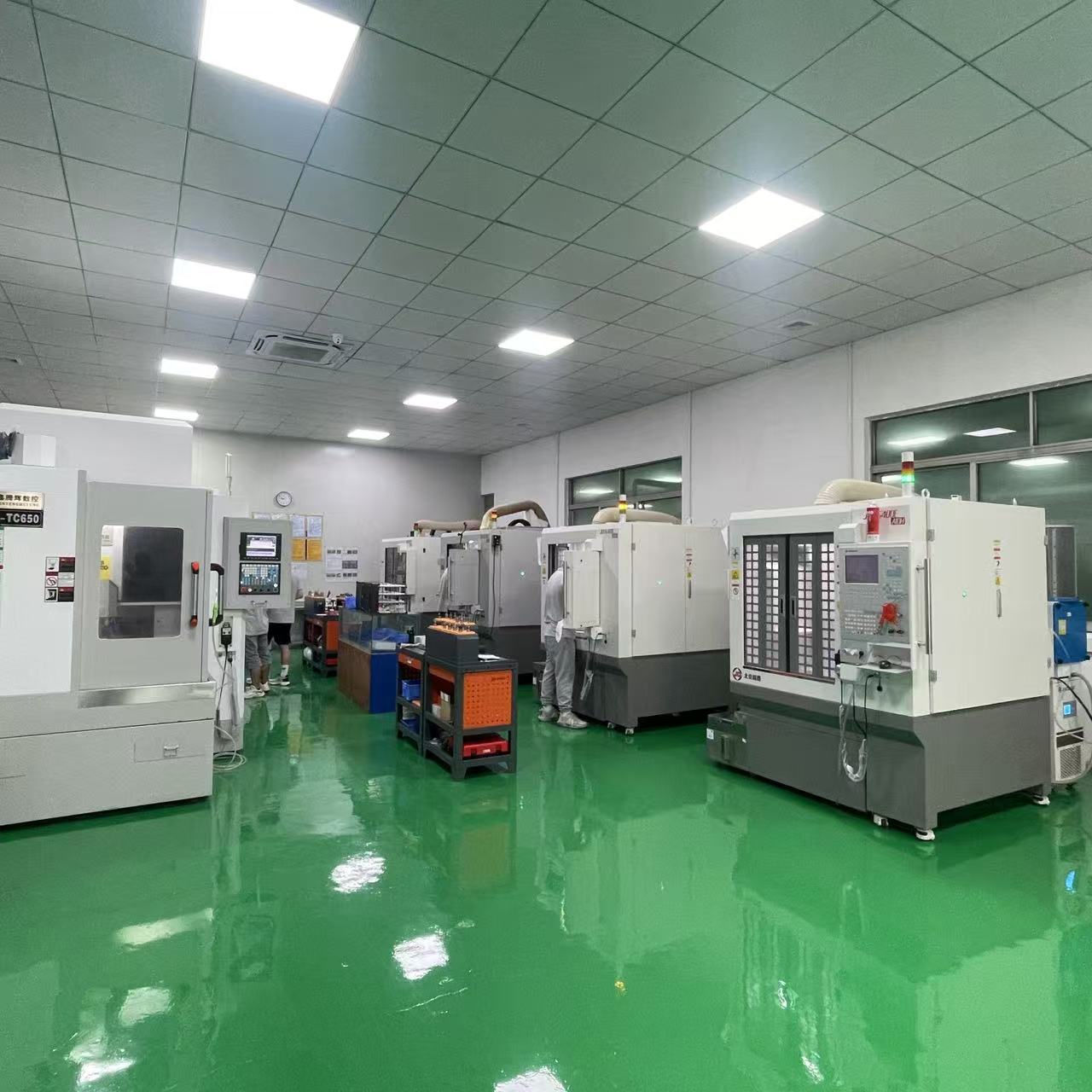
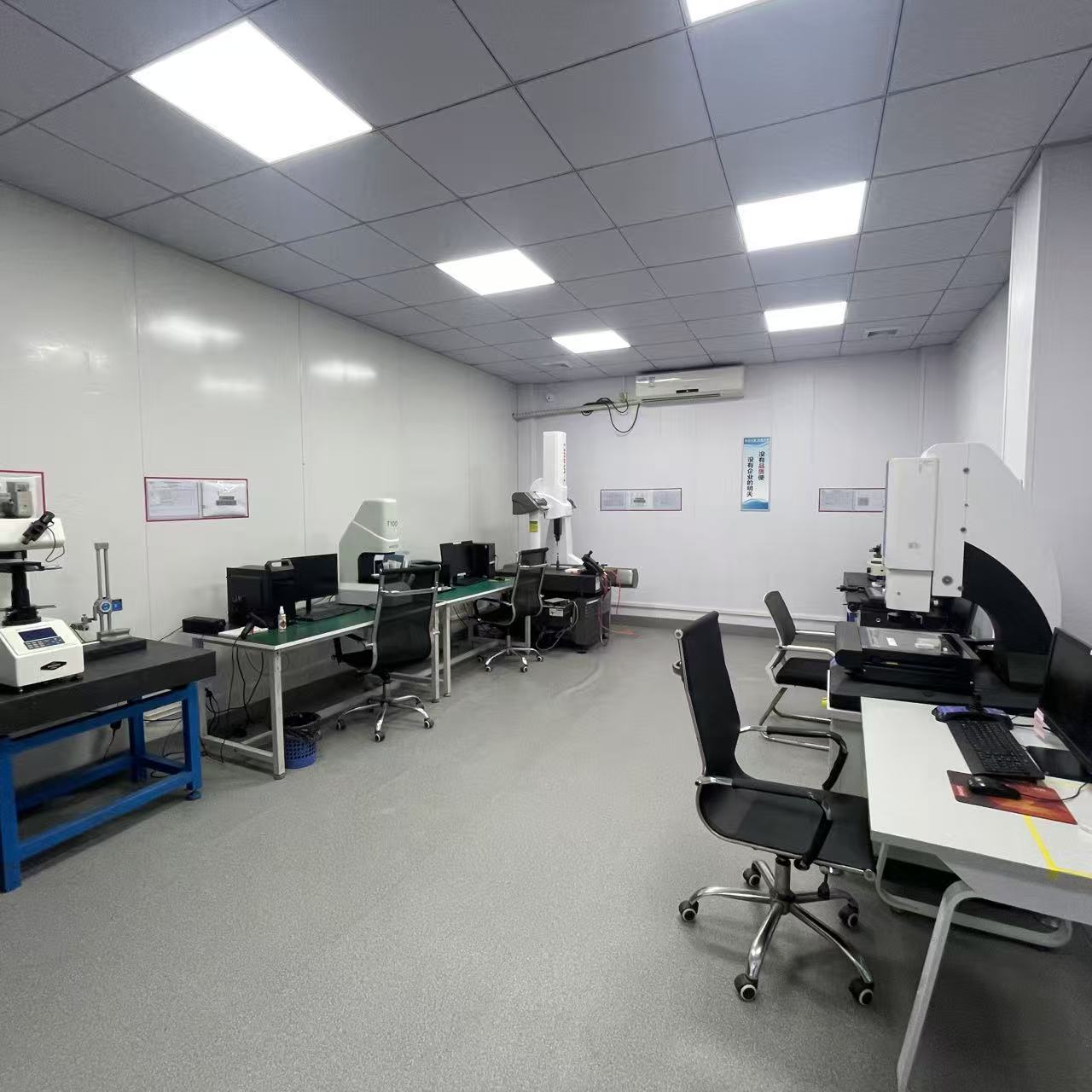
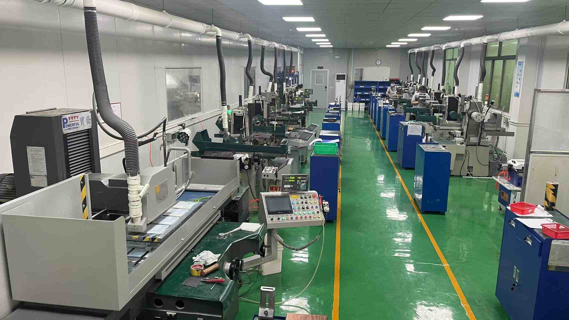
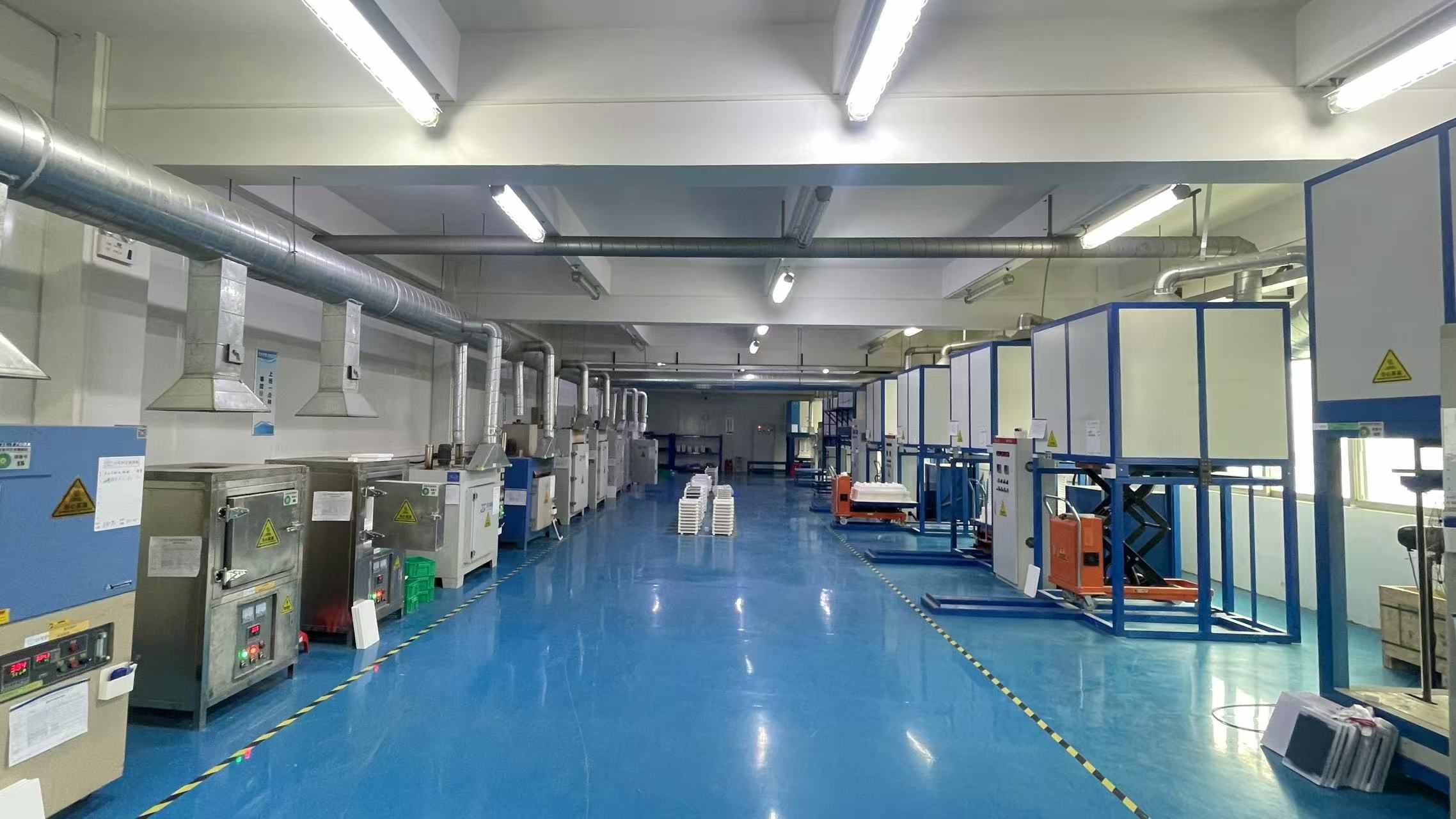
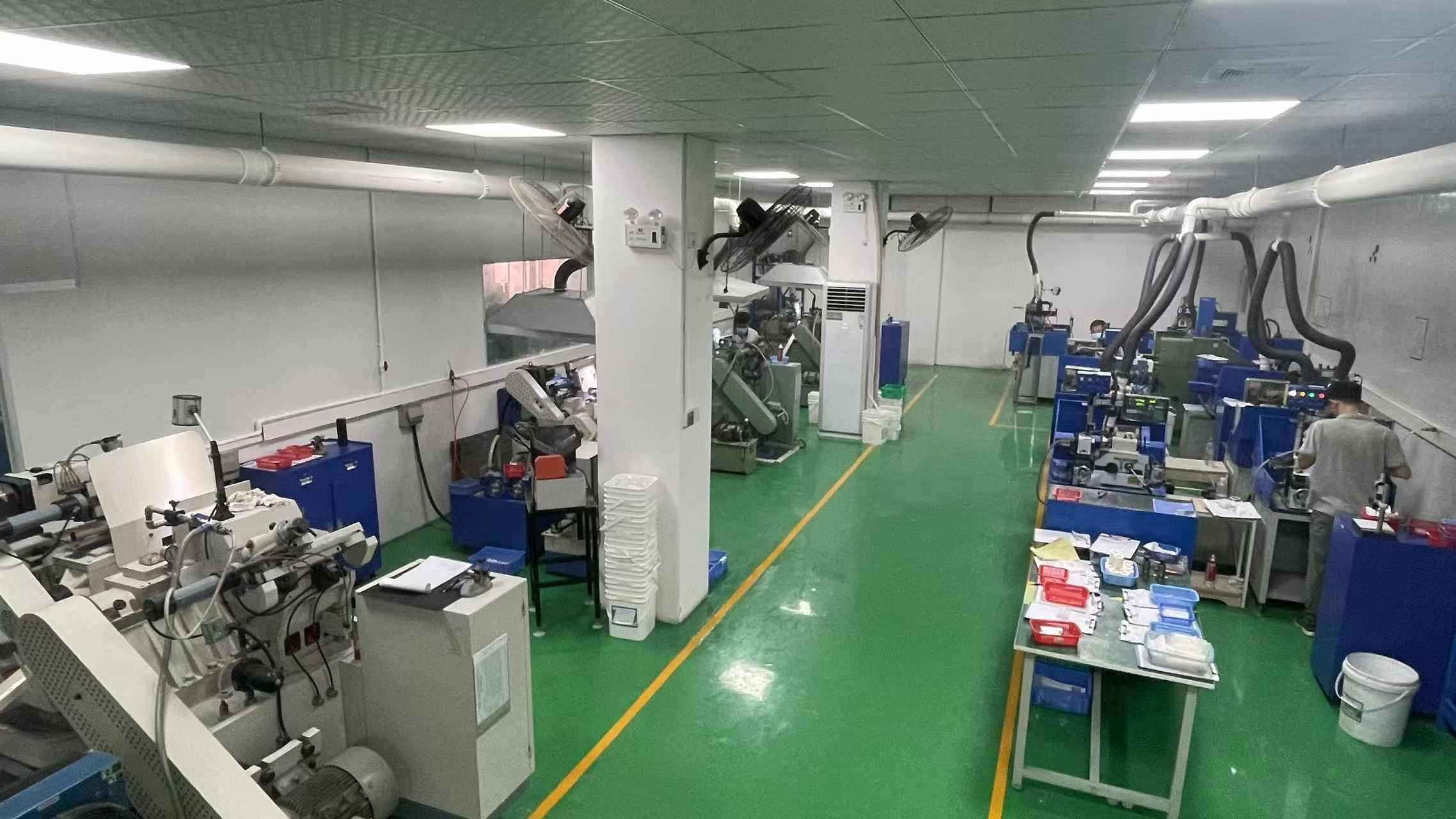
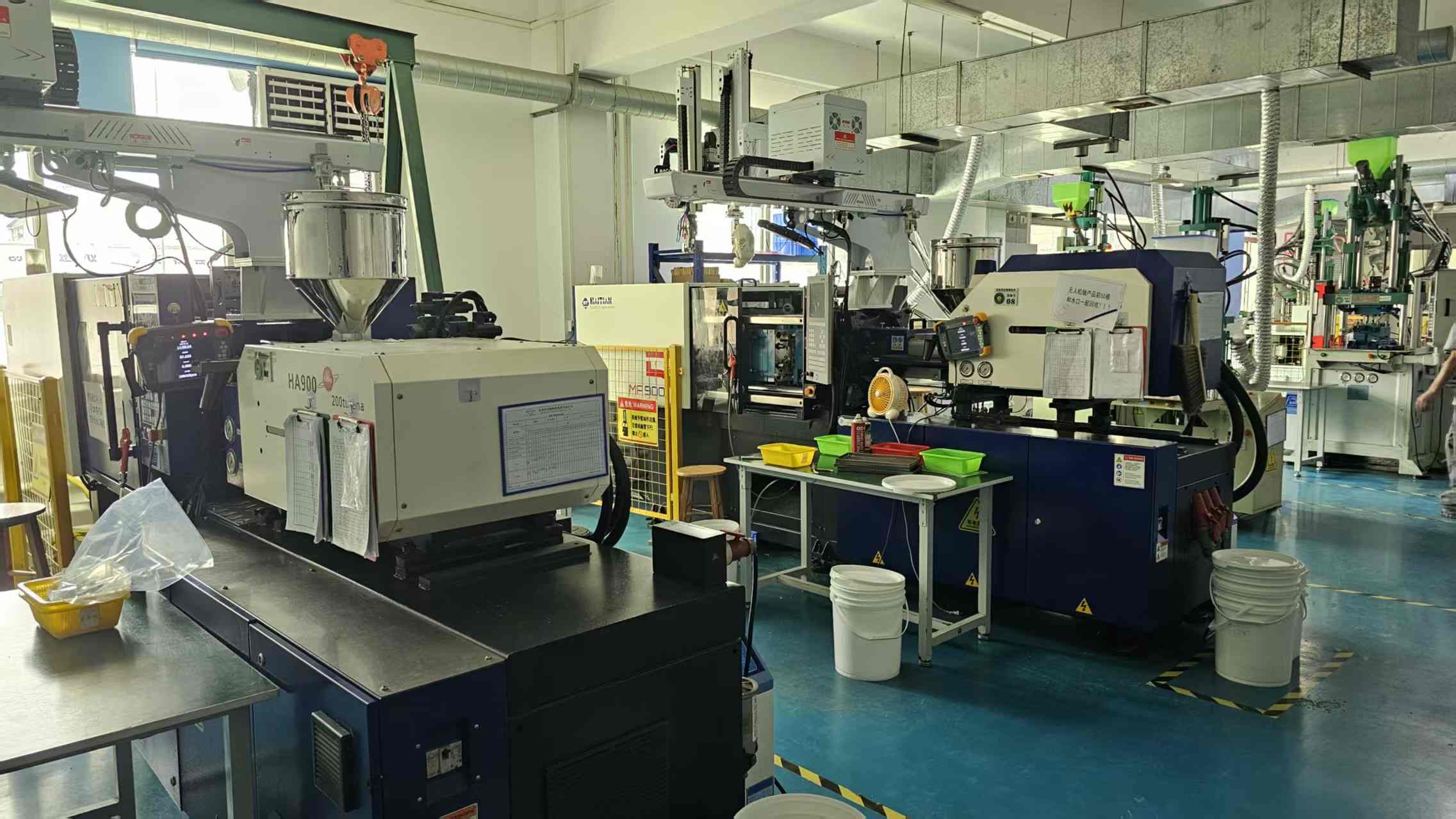
Our workshop
|
CNC Workshop |
Testing Room |
|
Surface grinding Workshop |
Sintering Workshop |
|
Circular Grinding Workshop |
Injection molding Machine Workshop |
Why choose us?
1.Customized R&D, rather than standard product adaptation
2.Deep control of materials science:Material Selection Based on Needs,Microstructure Optimization,Batch Consistency
3.Precision machining capability:Flatness can reach 0.001mm, parallelism 0.002mm, and roughness Ra 0.1μm.
FAQ
Q1: What products does your company offer?
We specialize in high-performance ceramics such as alumina and silicon nitride, providing insulators, structural components, wear-resistant parts, and customized solutions.
Q2: Can you customize non-standard parts?
Yes. We support processing based on provided drawings and collaborative technical development, offering a full-process service from design to mass production.
Q3: What about accuracy and delivery time?
Standard tolerance ±0.05mm, precision grade ±0.01mm; samples 7-15 days, bulk orders 20-30 days.
Q4: Main application areas?
Power, electronics, machinery, chemical, and aerospace industries.
Q5: Quality assurance measures?
Full-process quality inspection, providing material reports and performance test data, supporting third-party certification and testing.
Q6: Do you provide technical support?
We provide professional support such as material selection consultation, design optimization, and failure analysis.



 IPv6 network supported
Leave A Message
Scan to Wechat :

Scan to WhatsApp :