Leave A Message
If you are interested in our products and want to know more details,please leave a message here,we will reply you as soon as we can.


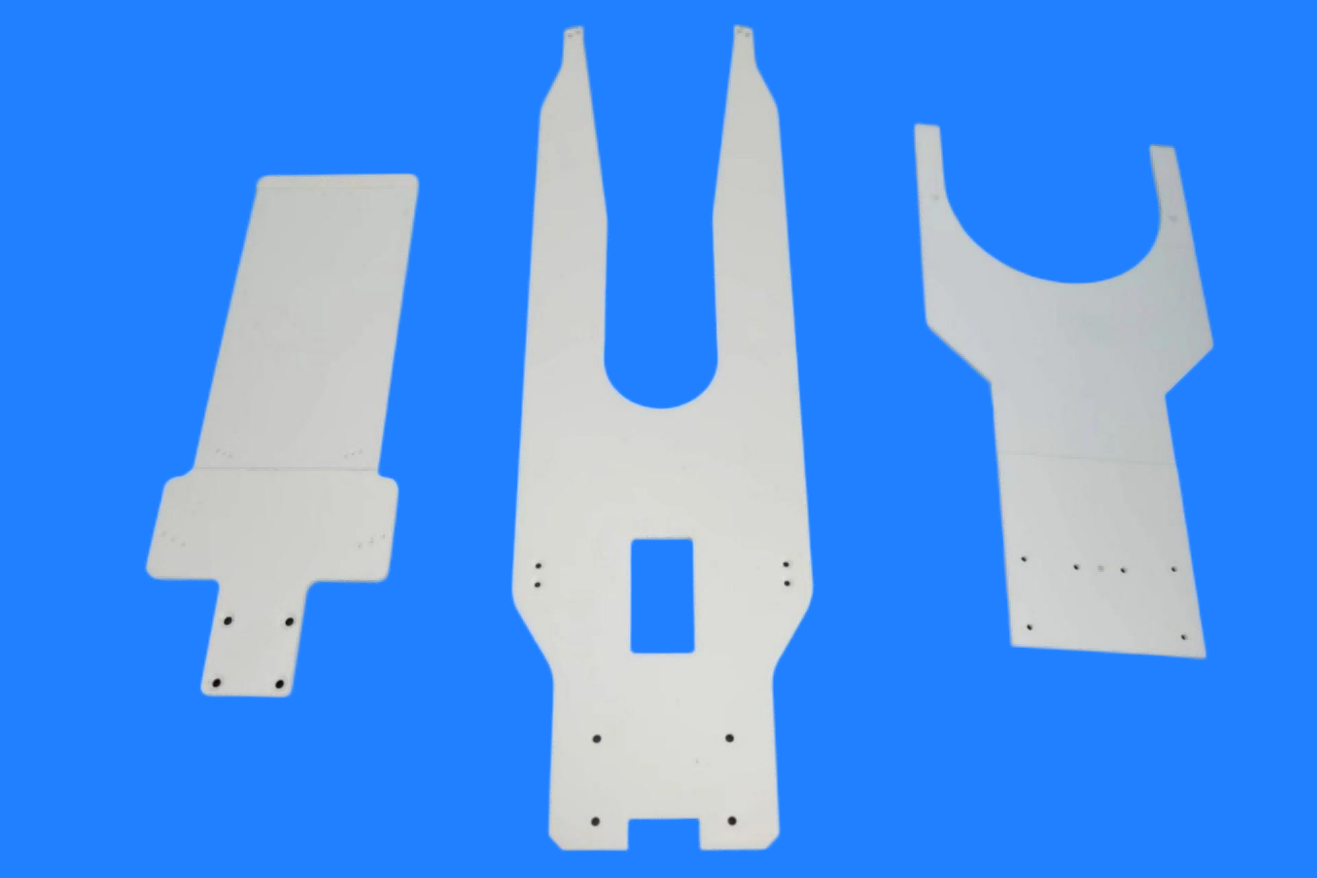
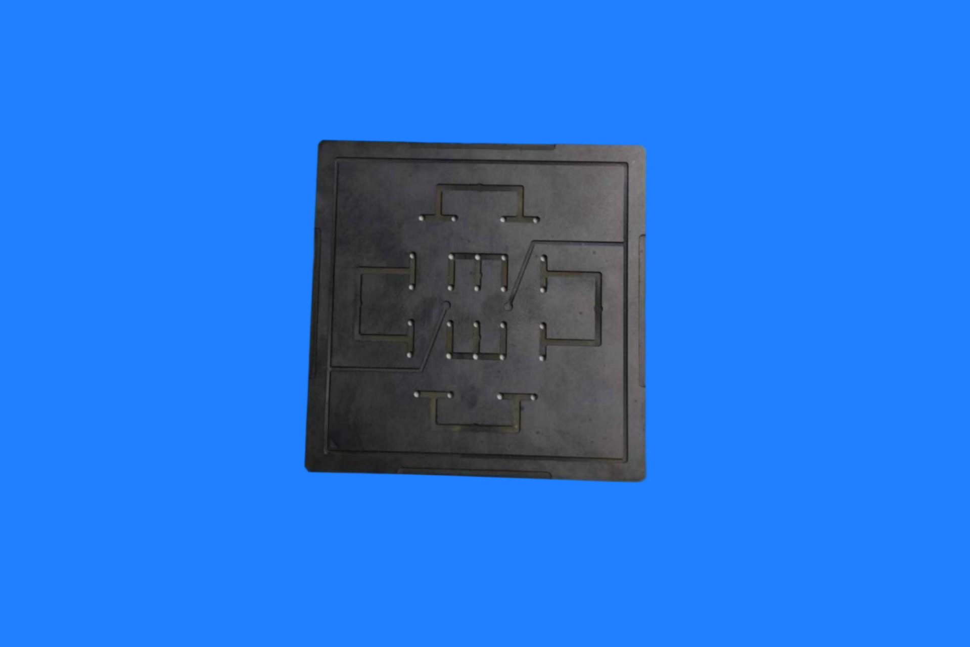
High Rigidity Silicon Carbide Ceramic Vacuum Chuck for Photovoltaic Equipment
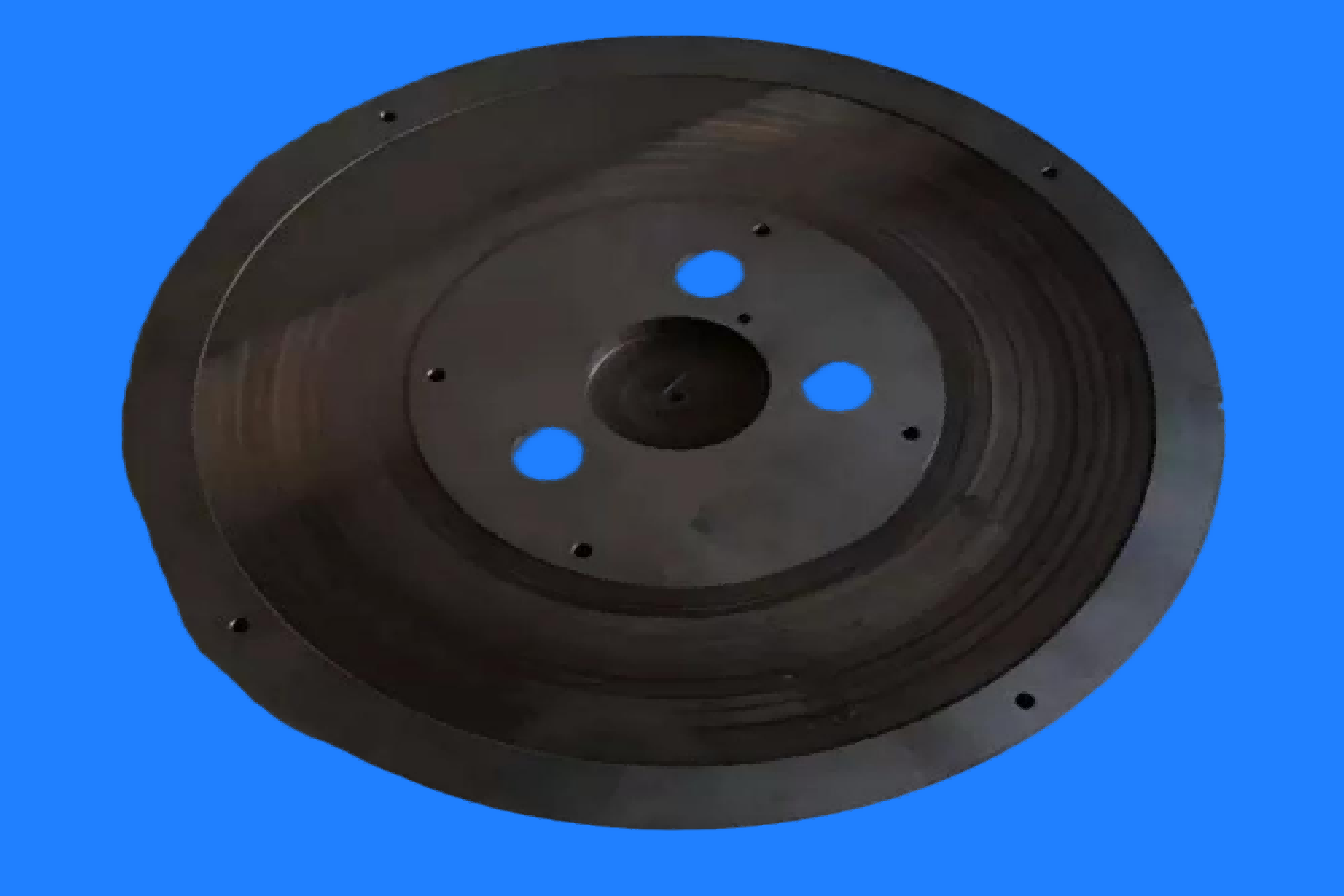
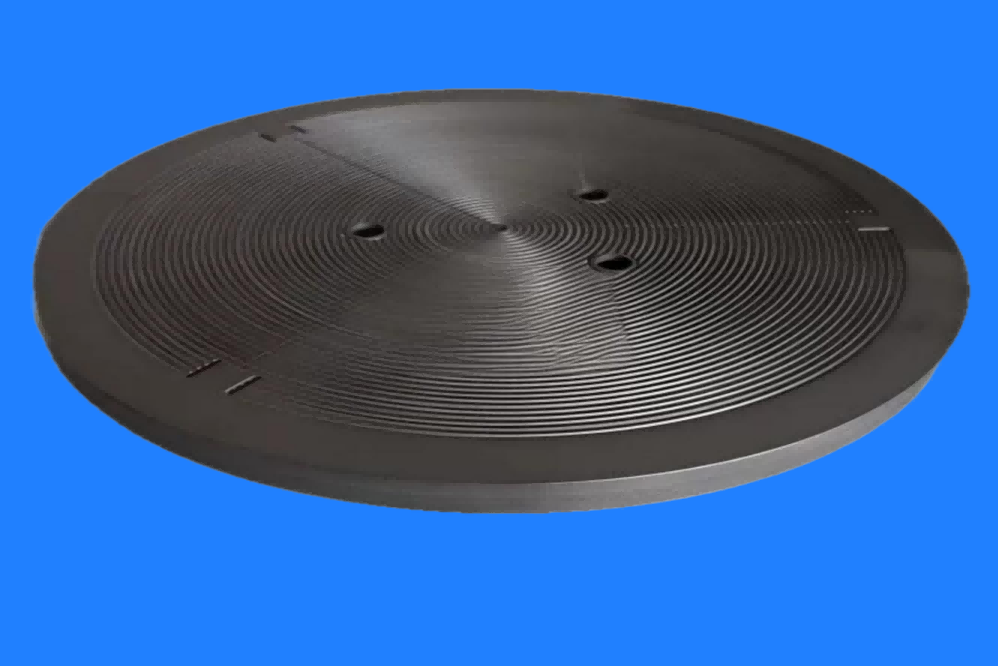
As critical components in semiconductor manufacturing equipment, the performance of SiC vacuum chucks directly determines the precision, yield, and efficiency of wafer processing. As wafer sizes increase and process nodes shrink, increasingly stringent demands are placed on the precision, thermal stability, and cleanliness of vacuum chucks. Thanks to their comprehensive advantages—high rigidity, high thermal conductivity, low thermal expansion, ultra-cleanliness, and wear resistance—SiC ceramics have become the material of choice for vacuum holding systems in high-end semiconductor equipment.
High Rigidity Silicon Carbide Ceramic Vacuum Chuck for Photovoltaic Equipment
Product Description
High Rigidity SiC Ceramic Vacuum Chucks are high-precision components designed to hold and secure wafers or workpieces in sectors such as semiconductor manufacturing, precision optical processing, optoelectronic displays, and advanced packaging. Manufactured from high-purity pressureless sintered silicon carbide (SSiC) or reaction-bonded silicon carbide (RBSiC) using precision molding, high-temperature sintering, and ultra-precision grinding and polishing processes, these chucks ensure the safe, stable, and damage-free holding of wafers—even in demanding cleanroom environments and under high-temperature processing conditions. Compared to traditional metal vacuum chucks, SiC ceramic chucks offer significant advantages, including high rigidity, low thermal expansion, excellent thermal conductivity, wear and corrosion resistance, and minimal particle generation; consequently, they have become essential components in 8-inch and 12-inch wafer manufacturing equipment.
Key Material Properties
As a representative third-generation semiconductor ceramic material, silicon carbide ceramic possesses the following outstanding properties:
| Performance Indicators | Typical Values | Functional Significance |
| Vickers Hardness | 20–25 GPa | high wear resistance, extending service life for repeated loading and unloading. |
| Modulus of Elasticity | 410–450 GPa | high rigidity, reducing vibration and mechanical drift. |
| Thermal Conductivity | 120–200 W/(m·K) | rapid temperature equalization; stabilizes wafer temperature. |
| Coefficient of Thermal Expansion | 4.0 × 10⁻⁶ /K (similar to silicon) | maintaining dimensional accuracy under temperature fluctuations |
| Maximum Operating Temperature | >1000°C | suitable for processes such as high-temperature annealing and CVD. |
| Chemical Stability | acid and alkali resistant, plasma resistant | suitable for corrosive environments such as etching and cleaning. |
| Resistivity | 10⁶–10⁸ Ω·cm (tunable) | anti-static; prevents ESD damage. |
Product Structure Type
Based on the method of vacuum clamping, silicon carbide ceramic vacuum chucks are primarily categorized into the following three structural types:
1. Pin Chuck
Features an array of precision-machined micro-pins on the surface; the wafer contacts the tops of the pins, while the gaps between them form vacuum channels. This design enables simultaneous vacuum clamping and backside helium cooling, with pin height tolerances controlled within ±0.1–2 μm. It is suitable for lithography and metrology/inspection processes that require backside cooling.
2. Groove Chuck
Features concentric or spiral vacuum grooves machined into the surface. This design offers a simple structure and reliable sealing, making it particularly well-suited for wafers with warpage exceeding 50 μm. Groove machining precision is controlled within ±10 μm.
3. Porous Chuck
Achieves uniform clamping through interconnected, micron-scale pores within the material, allowing the entire working surface to act as the clamping area; clamping force uniformity can reach within ±1%. Free from mechanical grooves or pin structures, it is ideal for ultra-thin wafers and compound semiconductor substrates, effectively preventing breakage caused by stress concentration.
Key Technical Parameters
| Parameter Items | Technical Specifications |
| Flatness | ≤ 0.2–1 μm (entire area) |
| Parallelism | ≤ 1–3 μm |
| Surface Roughness | Ra ≤ 0.02–0.1 μm |
| Pin Height | 0.05–0.2 mm |
| Pin Diameter (minimum) | Φ0.2 mm |
| Pin Pitch (minimum) | 2.5–3 mm |
| Annular Ring Width (minimum) | 0.4–0.7 mm |
| Thickness Tolerance | ±0.005–0.01 mm |
| Diameter Tolerance | ±0.01 mm |
| Applicable Wafer Specifications | 6-inch / 8-inch / 12-inch / 6/8-inch compatible / 8/12-inch compatible |
| Side Hole Feature | monoblock machining; minimum hole diameter 3 mm, maximum length 170 mm |
Product Core Competitive Advantages
1. Ultra-high precision and stability
Flatness ≤1 μm, ensuring the wafer surface remains within the optical focal plane
High elastic modulus (410–450 GPa) effectively suppresses machining vibrations and mechanical drift
Coefficient of thermal expansion matched to silicon wafers; deformation <0.3 μm under temperature fluctuations
2.Superior thermal management performance
Thermal conductivity of up to 120–200 W/(m·K) enables rapid dissipation of process heat
Backside helium cooling design ensures uniform wafer temperature control
Maintains mechanical strength and dimensional stability in high-temperature environments exceeding 1000°C
3.Ultra-clean and low-contamination
High-purity ceramic material with no metal ion leaching, preventing wafer contamination
Dense sintered structure minimizes particle generation, meeting Class 1 cleanroom requirements
Finely polished surface prevents scratching the backside of the wafer
4.Exceptionally long service life
Vickers hardness of 20–25 GPa; wear resistance far superior to metal suction cups
Resistant to acid/alkali corrosion and plasma bombardment; suitable for harsh processes such as etching and cleaning
Excellent surface shape retention and long intervals between reconditioning; reduces total cost of ownership by over 40%
5.High reliability and safety
Resistivity adjustable to the 10⁶–10⁸ Ω·cm range, effectively eliminating static charge accumulation
Uniform distribution of suction force, preventing wafer warpage or breakage caused by localized stress concentration
Reliable vacuum sealing, ensuring wafer safety and stability during handling and processing
Product Applications
1. Semiconductor Wafer Manufacturing
Widely used in core process steps such as photolithography, etching, CMP (Chemical Mechanical Polishing), thin-film deposition (CVD/PVD), wafer cleaning, and metrology/inspection. It is particularly well-suited for the precision processing of thin wafers, warped wafers, and compound semiconductor substrates (GaAs, SiC, sapphire).
2.Advanced Packaging
Used in wafer-level packaging (WLP), 3D packaging, and fan-out packaging for operations such as wafer bonding, reflow soldering, and temporary bonding, ensuring high-precision alignment and stable fixation.
3.Optoelectronic Display Manufacturing
Used to securely hold glass substrates during LCD/OLED panel production; its superior flatness and uniform suction ensure precision in film deposition and patterning.
4.Precision Inspection and Metrology
Used in precision measurement equipment—such as systems for optical inspection, film thickness measurement, OCD measurement, topography measurement, and defect detection—to ensure high-precision positioning of the workpieces being measured.
5.Emerging Technology Sectors
With the advancement of emerging technologies such as quantum computing, MEMS (Micro-Electro-Mechanical Systems), and advanced photonics, silicon carbide vacuum chucks are becoming indispensable precision handling solutions for these cutting-edge fields, thanks to their ultra-clean, thermally stable, and mechanically precise characteristics.
Customization Capabilities
We offer comprehensive custom design and manufacturing services tailored to specific customer requirements:
All products are manufactured, cleaned, and packaged in Class 10 (ISO 4) cleanroom environments to ensure delivery with zero particle contamination.
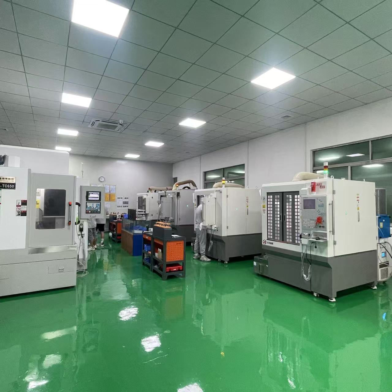
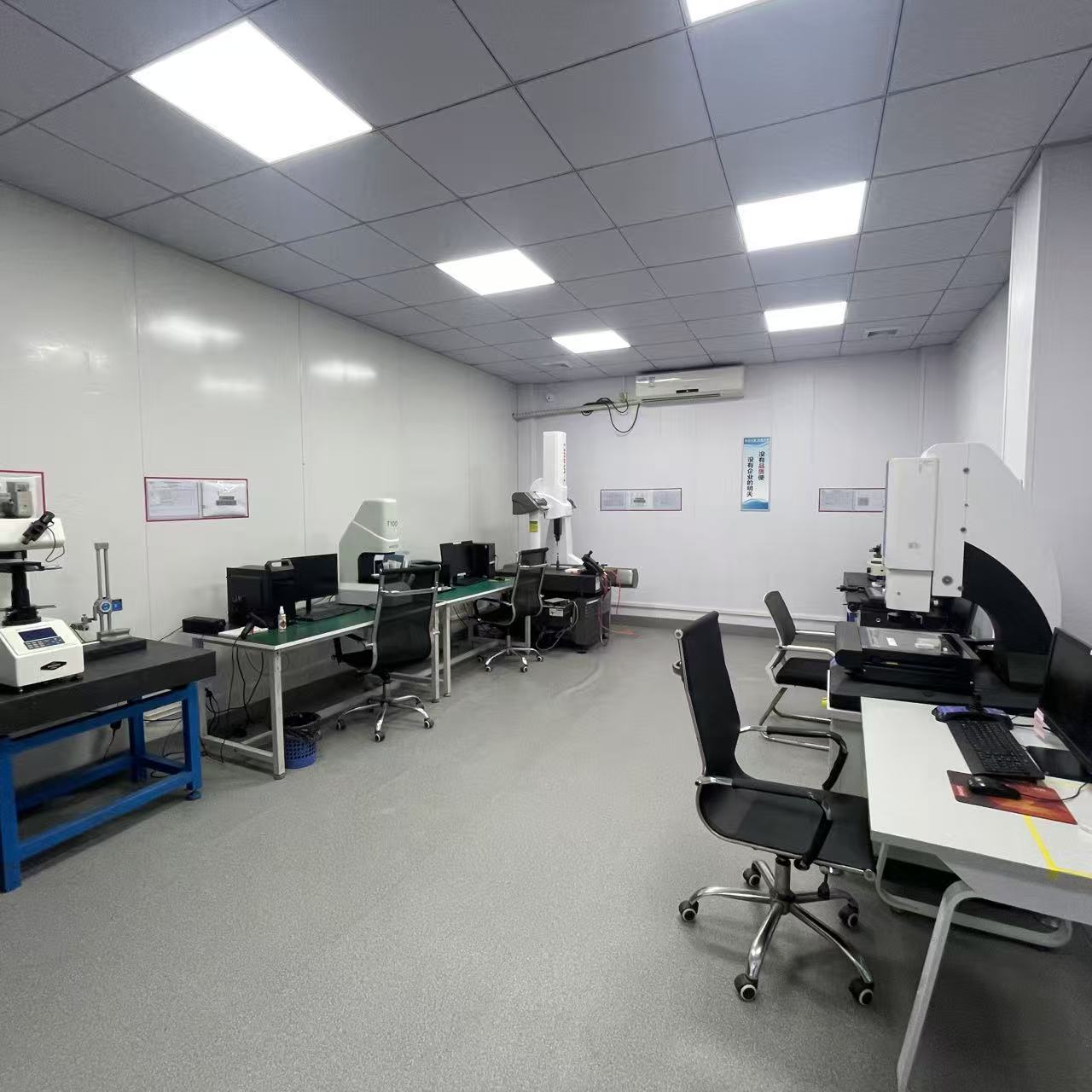
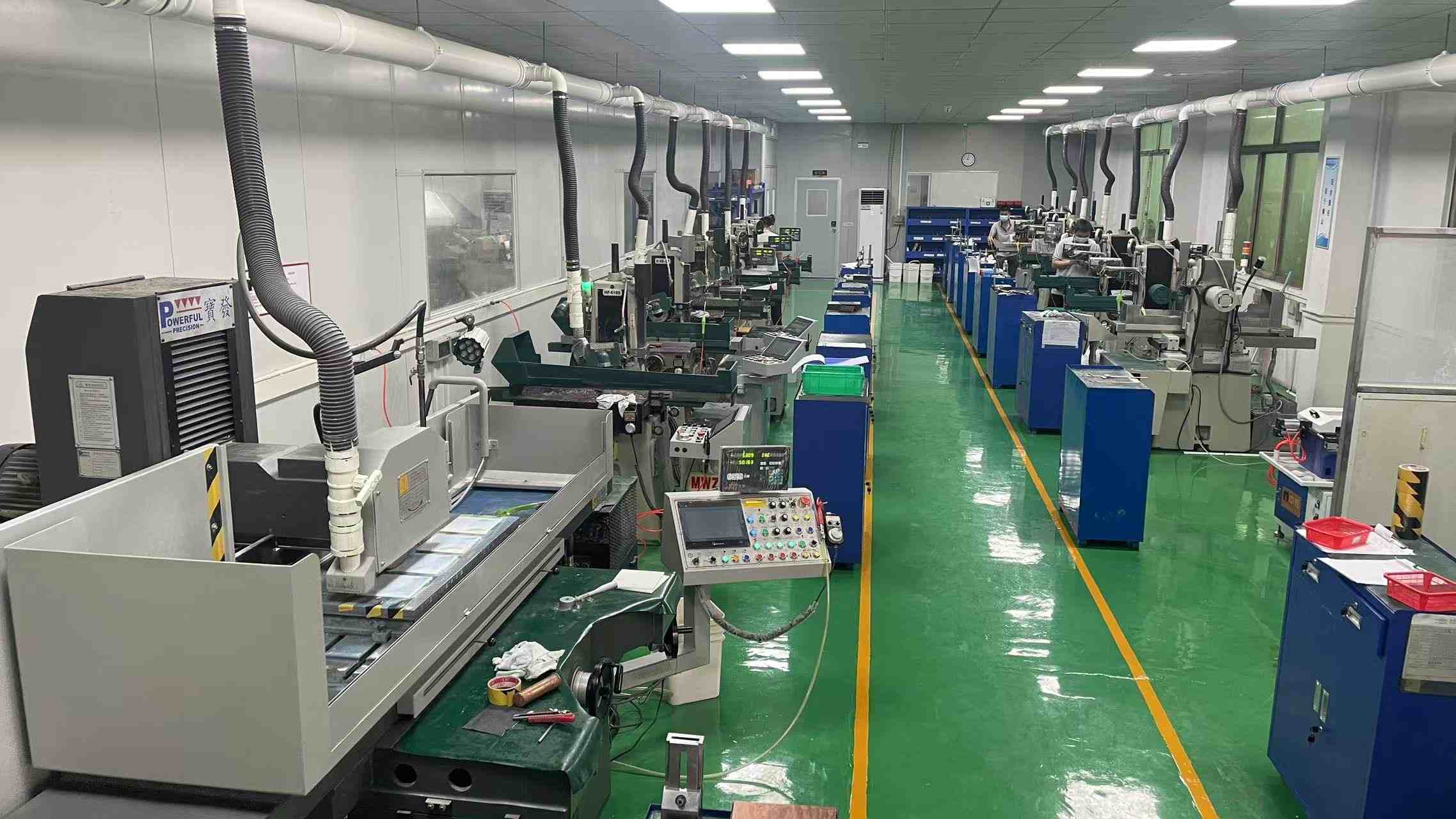
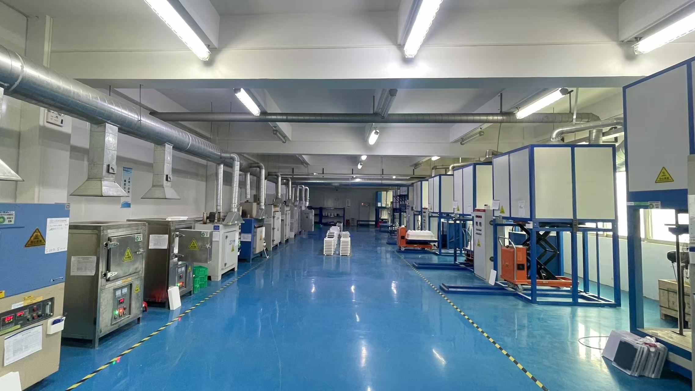
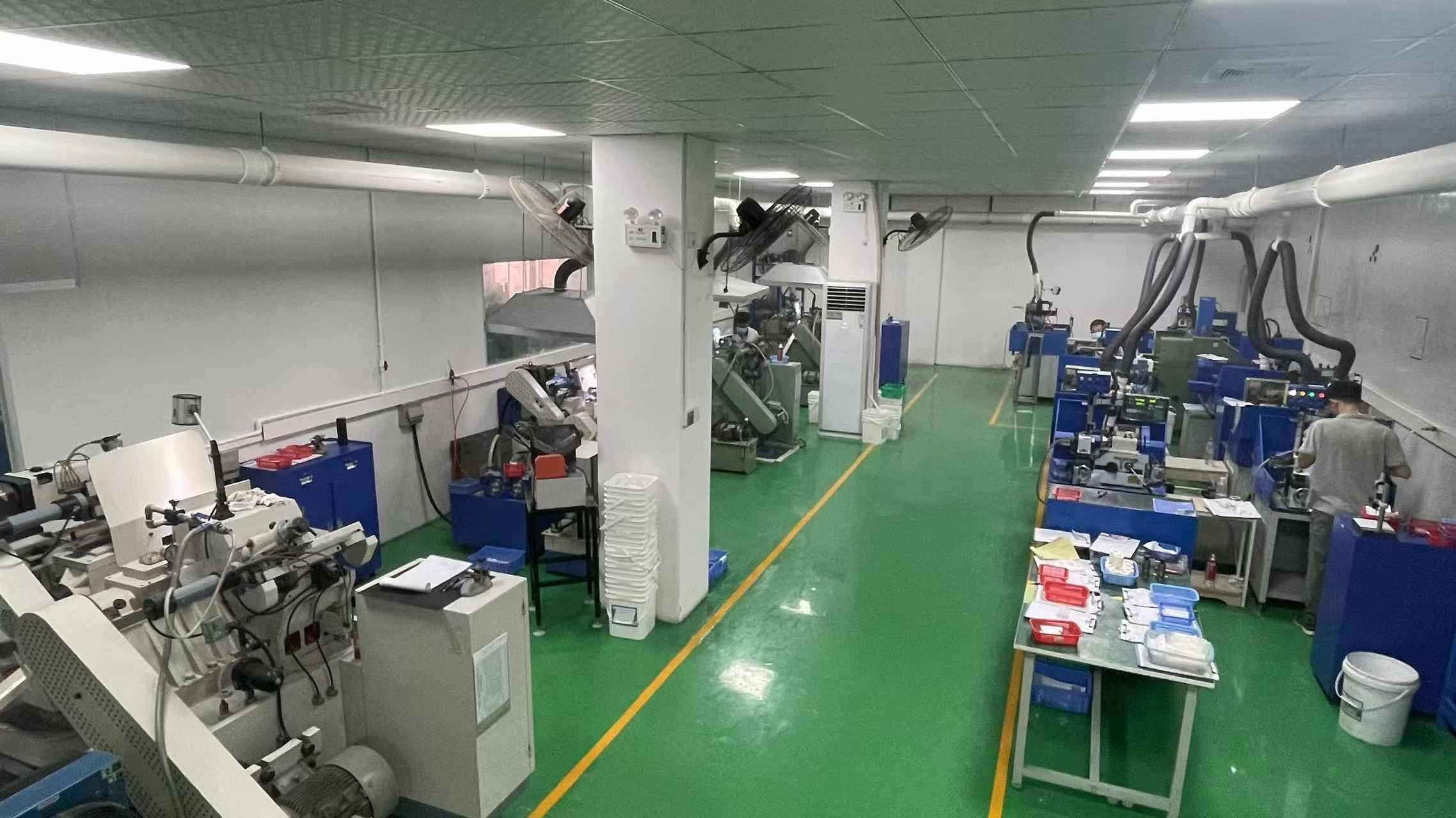
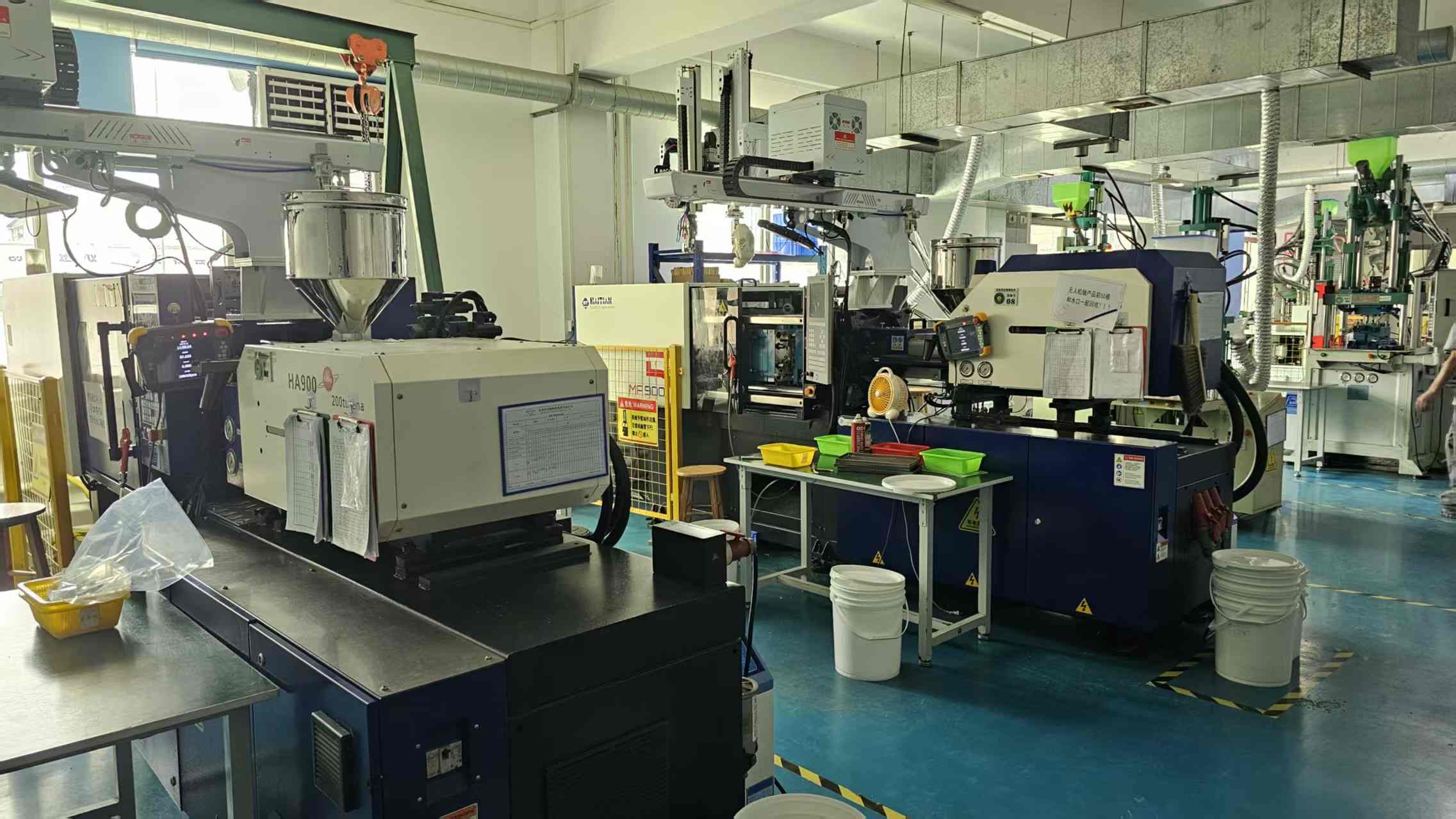
Our workshop
|
CNC Workshop |
Testing Room |
|
Surface grinding Workshop |
Sintering Workshop |
|
Circular Grinding Workshop |
Injection molding Machine Workshop |
Why choose us?
1.Customized R&D, rather than standard product adaptation
2.Deep control of materials science:Material Selection Based on Needs,Microstructure Optimization,Batch Consistency
3.Precision machining capability:Flatness can reach 0.001mm, parallelism 0.002mm, and roughness Ra 0.1μm.
FAQ
Q1: What products does your company offer?
We specialize in high-performance ceramics such as alumina and silicon nitride, providing insulators, structural components, wear-resistant parts, and customized solutions.
Q2: Can you customize non-standard parts?
Yes. We support processing based on provided drawings and collaborative technical development, offering a full-process service from design to mass production.
Q3: What about accuracy and delivery time?
Standard tolerance ±0.05mm, precision grade ±0.01mm; samples 7-15 days, bulk orders 20-30 days.
Q4: Main application areas?
Power, electronics, machinery, chemical, and aerospace industries.
Q5: Quality assurance measures?
Full-process quality inspection, providing material reports and performance test data, supporting third-party certification and testing.
Q6: Do you provide technical support?
We provide professional support such as material selection consultation, design optimization, and failure analysis.



 IPv6 network supported
Leave A Message
Scan to Wechat :

Scan to WhatsApp :