Leave A Message
If you are interested in our products and want to know more details,please leave a message here,we will reply you as soon as we can.


Ultra-high Thermal Conductivity Aluminum Nitride Ceramic Substrates Manufacturers
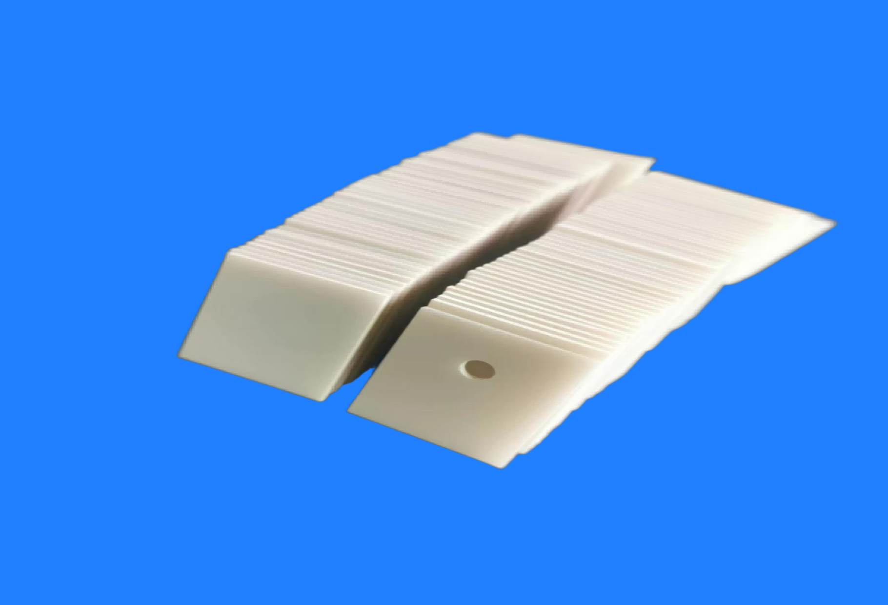
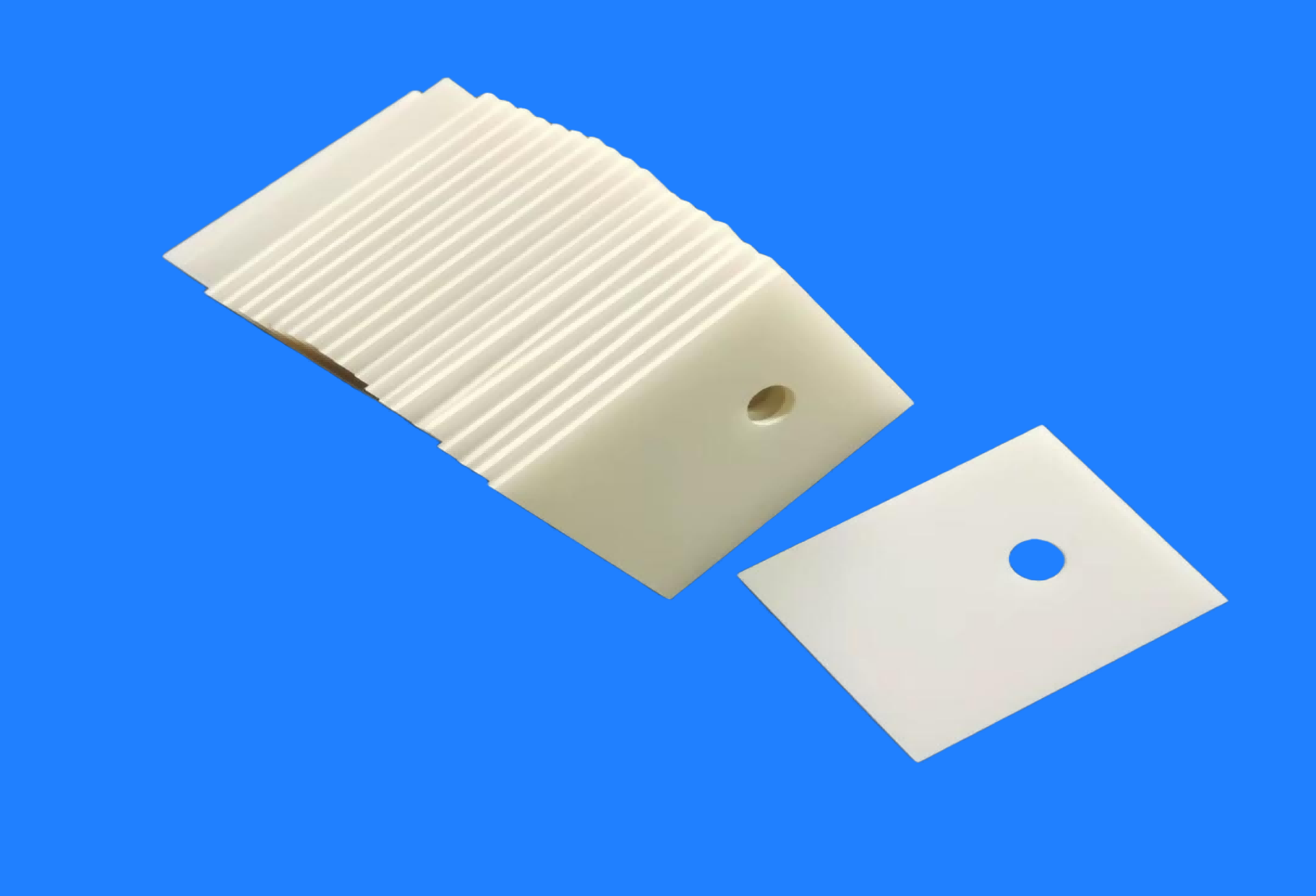
AlN Ceramic Substrates are functional electronic substrates manufactured from high-purity aluminum nitride powder using processes such as tape casting and high-temperature sintering. Thanks to their exceptional thermal conductivity and a CTE that closely matches silicon chips, AlN substrates have become the ideal choice for thermal management in high-power, high-density electronic devices, finding widespread application in power electronics, optoelectronics, RF communications, and new energy vehicles.
Ultra-high Thermal Conductivity Aluminum Nitride Ceramic Substrates Manufacturers
Product Description
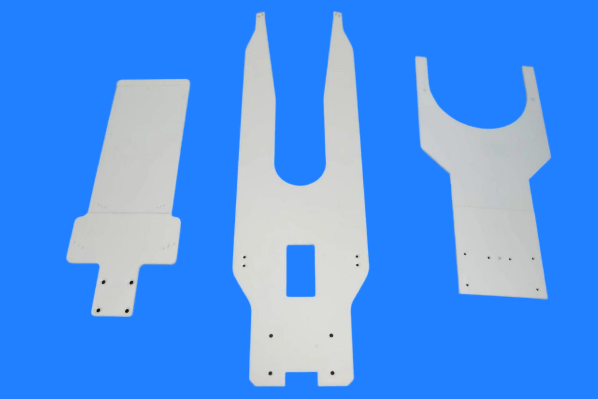
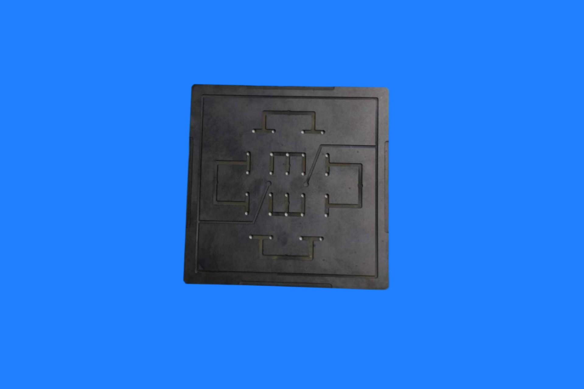
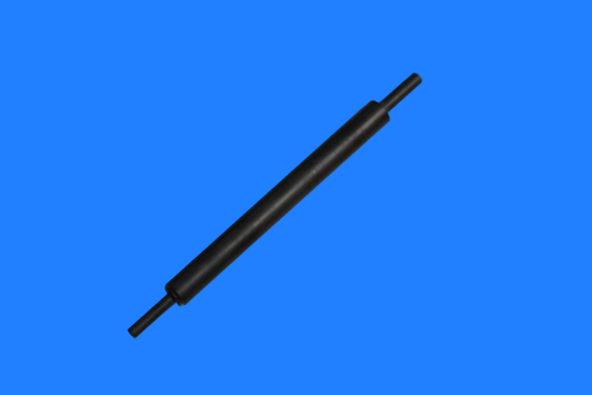
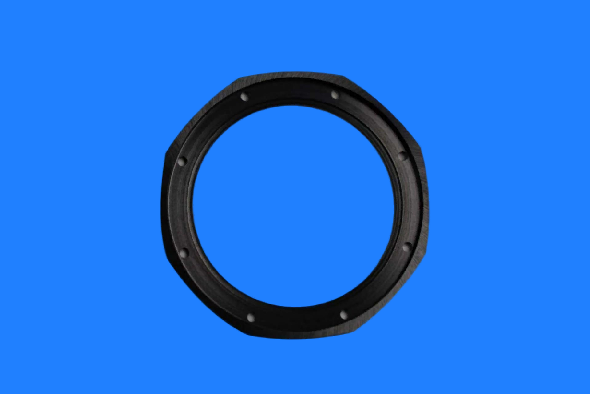
Our Aluminum Nitride Ceramic Substrates and custom-shaped components are engineered for applications demanding high thermal loads, high voltage, and high reliability. With a thermal conductivity of 170–230 W/(m·K)—approximately 7 to 10 times that of alumina—they efficiently dissipate heat from power devices while maintaining superior electrical insulation (>10¹⁴ Ω·cm). Their coefficient of thermal expansion (CTE) closely matches that of silicon, minimizing thermal stress at the die-attach and bonding interfaces and thereby extending module lifespan. These fully dense, RoHS-compliant, and beryllium-free products operate reliably at temperatures exceeding 800°C and in environments involving intense plasma or chemical corrosion. We offer polished substrates, metallized substrates (compatible with DPC, AMB, and DBC processes), and fully customized shaped components (featuring holes, slots, and stepped geometries) manufactured to precise specifications, with strict control over dimensions and warpage. When your application requires higher power, greater reliability, or a slimmer profile, AlN is the substrate material that enables you to achieve your goals.
Core Product Advantages
1.Exceptional Thermal Conductivity
The theoretical thermal conductivity reaches 320 W/(m·K), while actual products typically achieve 170–200 W/(m·K) or higher—5 to 10 times that of alumina (Al₂O₃) ceramics.It rapidly dissipates heat from the chip, significantly lowering device junction temperatures and enhancing the reliability and lifespan of power devices.
2.Coefficient of Thermal Expansion Matched to the Chip
With a coefficient of thermal expansion of approximately 4.5–5.5 × 10⁻⁶/K, it is highly compatible with silicon (Si) chips (approx. 4.2 × 10⁻⁶/K).It effectively alleviates thermal cycling stress, preventing solder layer cracking and chip detachment, making it particularly suitable for high-power applications subject to frequent thermal cycling.
3..Excellent electrical insulation properties
It features high volume resistivity (>10¹⁴ Ω·cm), a dielectric strength exceeding 15 kV/mm, and high breakdown voltage. With a low dielectric constant (approximately 8.8) and low dielectric loss, it is suitable for high-frequency and high-voltage applications.
4.Excellent mechanical and chemical properties
High flexural strength (>300 MPa), high hardness, and resistance to wear and pressure.Chemically stable, non-toxic, and compliant with RoHS environmental standards; free from toxic substances such as BeO, making it a safe alternative to toxic beryllium oxide (BeO) substrates.
5.Excellent high-temperature resistance
Wide normal operating temperature range (-40°C to 600°C), good thermal stability, and resistance to performance degradation.
Common Product Specifications
Standard sizes: 50×50, 100×100, 114×114 (4.5”), 139.7×190.5 (5.5”×7.5”) mm; Thickness: 0.25/0.38/0.5/0.635/0.75/1.0/1.5/2.0 mm;
Customization options include drilling, slotting, stepped features, and irregular shaping—all manufactured according to drawings.
Key Technical Parameters (Typical Values)
| Item | Typical Indicators |
| Thermal Conductivity | 170–200 W/(m·K) (up to 230+ for high-thermal-conductivity versions) |
| Coefficient of Thermal Expansion (20–300°C) | 4.5–5.5 × 10⁻⁶ /K |
| Dielectric Constant (1 MHz) | 8.5–8.8 |
| Dielectric Loss (1 MHz) | < 3 × 10⁻⁴ |
| Volume Resistivity | > 10¹⁴ Ω·cm |
| Dielectric Strength | ≥ 15 kV/mm |
| Flexural Strength | ≥ 300 MPa |
| Density | 3.26 g/cm³ |
| Common Thicknesses | 0.25–1.0 mm (customizable) |
| Standard Sizes | 4"×4", 6"×6", and custom specifications |
Product Types
1.AMB (Active Metal Brazing) Aluminum Nitride Substrates: Feature a copper layer brazed onto the AlN surface; offer high bond strength and high current-carrying capacity, making them the mainstream packaging solution for IGBT modules.
2.DBC (Direct Bonded Copper) Aluminum Nitride Substrates: Feature a copper layer directly bonded to the ceramic at high temperatures; offer low thermal resistance and a short thermal conduction path.
3.Thick-film/Thin-film Metallized Substrates: Suitable for metallized circuitry requirements in high-precision and high-frequency applications.
Typical Application Areas
Power Electronics: IGBT power modules, MOSFETs, rectifier modules, servo drives, PV inverters, energy storage converters (PCS)
New Energy Vehicles: motor controllers, on-board chargers (OBC), DC-DC converters, battery management systems
LED & Optoelectronics: high-power LED packaging, laser heat dissipation, UV curing equipment
RF & Communications: 5G base station power amplifiers, radar, microwave device substrates
Semiconductor Equipment: etching machines, heating and electrostatic chuck components for PVD/CVD equipment
Why Choose Us



 IPv6 network supported
Leave A Message
Scan to Wechat :

Scan to WhatsApp :