

Wafer Manufacturing and Heat Treatment

In the semiconductor manufacturing field, we provide a complete chain of high-performance ceramic component solutions, from wafer transport and positioning to high-temperature heat treatment. We understand that even micron-level contamination or dimensional fluctuations in the manufacturing process can directly affect chip yield. Therefore, we focus on providing customers with core components that maintain high cleanliness, high stability, and high precision even in extreme environments through material innovation and precision manufacturing.
1.Wafer Transfer and Positioning
Industry scenario: In wafer manufacturing, automated transfer and high-precision positioning place extremely high demands on cleanliness, chemical inertness, and dimensional stability. Any micron-level contamination, wear, or displacement can lead to a decrease in chip yield.
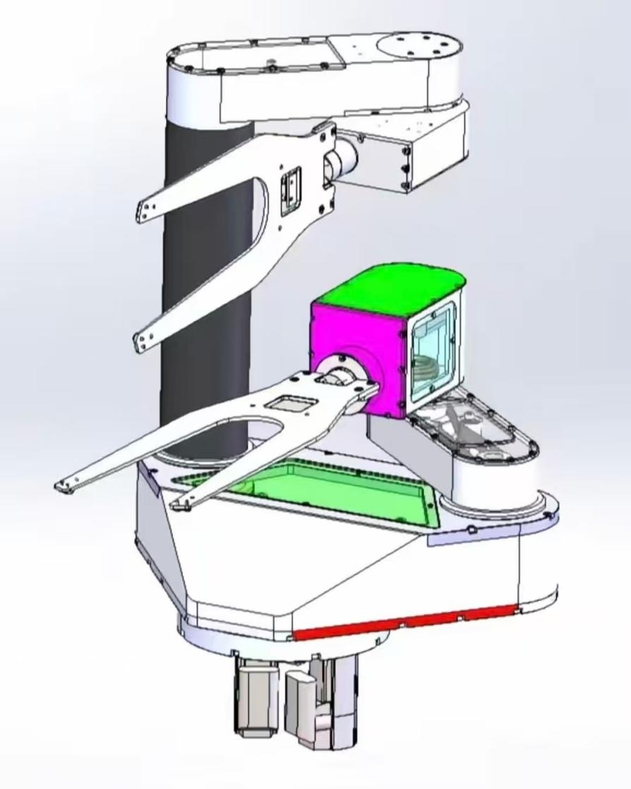
Ceramic Solutions: We offer Ceramic Wafer Robot Arm, electrostatic ceramic chucks (ESCs), precision ceramic guides, and positioning pins made from high-purity alumina, aluminum nitride, or silicon carbide. All components undergo precision polishing and rigorous cleaning to achieve ultra-clean surface standards and can be customized to meet specific equipment interface and load-bearing requirements.
Core Value: We directly solve the problems of positioning drift and product contamination caused by contamination, wear, or thermal expansion of transfer components. Our Ceramic Components possess intrinsic chemical inertness, ensuring zero contamination upon wafer contact; their ultra-high hardness and low coefficient of thermal expansion ensure consistently micron-level positioning accuracy even in high-speed motion and temperature-changing environments, thus supporting high repeatability and ultra-long service life of the equipment.
2.High-Temperature Heat Treatment Processes
Industry Scenarios: Heat treatment processes such as diffusion, oxidation, annealing, and chemical vapor deposition require high-temperature (up to 1300℃) and high-cleanliness environments. The process chambers and supporting components must possess excellent high-temperature stability, thermal shock resistance, and low outgassing characteristics to ensure process uniformity and equipment lifespan.
Ceramic Solutions: We provide a complete range of heat treatment consumables and components for horizontal and vertical furnace tubes, including high-temperature ceramic furnace tubes (quartz, silicon carbide coating), multi-groove ceramic boats, ceramic heat insulation baffles, suspending cores, and embedded ceramic heaters. Material systems include high-purity quartz, reaction sintering, and chemical vapor deposition silicon carbide to meet the temperature and cleanliness requirements of different processes.
Core Value: We effectively address process drift and particulate defects caused by high-temperature component deformation, outgassing contamination, and uneven thermal fields during heat treatment. Our ceramic components exhibit virtually no creep under prolonged high-temperature environments and possess an extremely low coefficient of thermal expansion, ensuring stable wafer spacing and uniform thermal field. Simultaneously, the material's low outgassing characteristics maintain a pure process atmosphere, fundamentally guaranteeing film uniformity and consistent doping concentration, and significantly extending maintenance cycles.
We are not merely a supplier of ceramic components, but also your material solutions partner for addressing the demanding challenges of semiconductor manufacturing. By deeply understanding your process pain points, we provide end-to-end support from material selection and structural design to surface treatment, safeguarding every nanometer of precision in your manufacturing process with the ultimate performance of our materials.
Thin Film Deposition Equipment

In thin film deposition (CVD, ALD) processes, we offer a full range of high-performance ceramic component solutions. Addressing the core needs of semiconductor equipment in high-temperature, highly corrosive, and high-precision environments, we provide comprehensive solutions from material design to component functionality, ensuring process stability and chip yield.
1. Wafer Adsorption and Precise Temperature Control
Industry Scenario: During thin film deposition, wafers need to be absolutely stable and precisely controlled at a set temperature (±0.1℃ accuracy). Traditional mechanical clamping or vacuum adsorption easily leads to backside contamination, particle generation, and thermal unevenness, directly affecting the uniformity of film thickness and properties.
Ceramic Solution: We offer electrostatic chucks (ESCs) made from high-purity aluminum nitride (AlN) material. This solution combines customized electrode design with precision ceramic processing technology to achieve contactless, stress-free wafer adsorption.
Core Value: Solving the problem of thin film uniformity caused by unstable adsorption or temperature unevenness for our customers. Our electrostatic chuck provides strong electrostatic attraction while leveraging the high thermal conductivity and insulation properties of aluminum nitride to achieve rapid temperature response and uniform distribution on the back side of the wafer, thereby ensuring the repeatability and yield of the deposition process.
2. Uniform Distribution of Reactive Gases and Stable Plasma Generation
Industry Scenario: The uniformity of reactant gas distribution within the chamber and the stability of the plasma are crucial for determining the consistency of film composition and thickness. Metal spray heads are susceptible to corrosion under long-term plasma bombardment, generating particles and altering the airflow field, leading to process drift and contamination.
Ceramic Solution: We offer aluminum alloy gas spray heads/upper electrodes coated with yttrium oxide (Y₂O₃) using anodizing or plasma spraying. This solution allows for optimized orifice and flow channel design based on the customer's process gases and power requirements.
Core Value: Solving process instability issues caused by component corrosion and contamination. Our ceramic-coated spray heads significantly enhance resistance to plasma corrosion, maintain long-term stable airflow distribution, and, as the upper electrode, ensure uniform and efficient plasma generation, extending maintenance intervals and reducing particle defects.
3. Rapid and Uniform Heating and High-Temperature Process Stability
Industry Scenario: Thin film deposition requires rapidly and uniformly heating wafers to process temperatures (typically 300-600℃) and maintaining stability during long-term processes. Traditional heaters suffer from slow thermal response, large temperature gradients, or material outgassing contamination.
Ceramic Solution: We offer heater substrates made of high-purity graphite with a dense chemical vapor deposition (CVD) silicon carbide (SiC) coating, or integrally dense sintered silicon carbide heaters.
Core Value: Solving problems of low heating efficiency, temperature unevenness, and potential contamination for our customers. Our solutions utilize the excellent thermal conductivity and high-temperature strength of silicon carbide to achieve rapid heating and excellent radial temperature uniformity. Its high purity and low outgassing characteristics further ensure the cleanliness of the process chamber, supporting more stringent process windows.
4. Long-Term Cavity Protection and Process Edge Uniformity Optimization Scenarios
Industry Scenarios: The metal inner walls of process cavities are continuously eroded in a plasma environment, and the detached particles contaminate the wafer; simultaneously, uneven plasma sheathing at the wafer edges leads to abnormal film edge thickness, affecting the effective chip area.
Ceramic Solutions:Cavity protection: we provide integral yttrium oxide (Y₂O₃) liners and protective sleeves formed by plasma spraying or sintering, achieving a tight fit with the cavity.
Edge Uniformity Optimization: we provide focusing rings precision-machined from high-purity quartz, alumina, or silicon nitride, with their shape and dielectric constant optimized for the customer's specific process.
Core Value: Solving Cavity Contamination and Lifespan Issues: The ceramic liner forms a corrosion-resistant barrier for customers, greatly reducing corrosion and particle generation in the metal cavity, extending the lifespan of the core cavity, and reducing spare parts costs.
Addressing edge uniformity issues: Customized focusing rings effectively improve thin film uniformity in wafer edges by optimizing the electric field and airflow distribution, thereby increasing die yield per wafer.
We are committed to being a reliable partner for semiconductor thin film deposition equipment manufacturers. We not only provide high-performance standardized ceramic components, but also offer one-stop customized solutions tailored to our customers' specific process requirements, from material selection and structural design to precision manufacturing, working together to meet the challenges of advanced processes.
Semiconductor etching machine

In semiconductor plasma etching equipment, we provide key ceramic component solutions. Addressing the extreme requirements of uniformity, precision, and cleanliness in etching processes, we ensure process stability and improve chip yield through precise material and structural design.
1. RF Energy Coupling and Plasma Generation
Industry Scenario: In etching equipment such as ICP, it is necessary to efficiently couple RF energy into the process cavity to generate high-density plasma, while simultaneously isolating the plasma from the external RF system. Traditional materials are susceptible to corrosion or energy loss at high power, affecting process stability.
Ceramic Solution: We offer dielectric windows/radomes precision-manufactured using high-purity quartz or aluminum nitride. This component, serving as the cavity top cover, has precise thickness and dielectric constant and can be customized to meet customer frequency and power requirements.
Core Value: We directly solve the problems of low RF energy coupling efficiency and short component lifespan. Our dielectric windows possess excellent dielectric properties and extremely high plasma corrosion resistance, ensuring efficient and stable RF energy transmission to the cavity, maintaining stable plasma density, and significantly extending the lifespan of key consumables, thus reducing equipment operating costs.
2. Precise Wafer Temperature Control and Fixation
Industry Scenario: In etching processes, wafer temperature is one of the core parameters affecting etching rate, selectivity, and critical dimension uniformity. Wafers need to be firmly fixed and precisely temperature-controlled, while withstanding the extreme environments of back-side helium cooling and front-side plasma bombardment.
Ceramic Solution: We offer electrostatic chucks made of aluminum nitride or alumina. This solution integrates multi-zone heating and back-side helium cooling channels, with precision-machined surfaces to ensure flatness and uniform adhesion.
Core Value: We effectively address the problems of poor etching uniformity and pattern defects caused by uneven wafer temperature or unstable adhesion. Our electrostatic chucks, with their excellent thermal conductivity and insulation properties, combined with a multi-zone temperature control design, achieve wafer surface temperature uniformity at the ±0.5℃ level; strong electrostatic adhesion ensures no wafer slippage during the process, providing stable thermal management and mechanical reference for advanced etching processes.
3. Edge Uniformity Control in Etching Processes
Industry Scenario: In plasma etching, due to uneven distribution of the electric field and gas flow at the edges, the etching rate and profile in the wafer edge region often differ from those in the center region. This directly affects the effective area and yield of the chip.
Ceramic Solution: We offer focusing rings precision-machined from materials such as aluminum nitride. Their shape, size, and dielectric constant can be optimized according to the customer's equipment model and specific process formulation.
Core Value: We specifically address the common industry challenge of uneven etching at wafer edges. Our customized focusing rings effectively control the etching rate in the edge region by optimizing the plasma sheath and reactive gas flow distribution at the wafer edge, significantly improving the etching uniformity of the entire wafer and thus increasing the number of usable chips per wafer.
We are committed to becoming a strategic partner for etching equipment manufacturers and chip factories, providing not only Standardized High-performance Ceramic Components, but also one-stop customized development from material formulation and simulation to precision manufacturing to address your most cutting-edge process challenges, jointly pushing the boundaries of etching process precision.
Leave A Message
Scan to Wechat :

Scan to WhatsApp :
